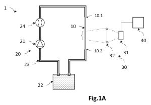
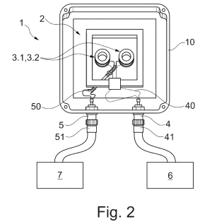
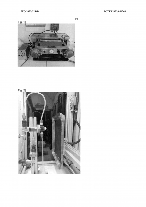
Procédé et dispositif de détermination d’une pression d’un liquide en écoulement dans un canal IRAMIS, LLB, MMB 29 décembre 2023
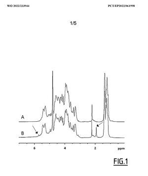
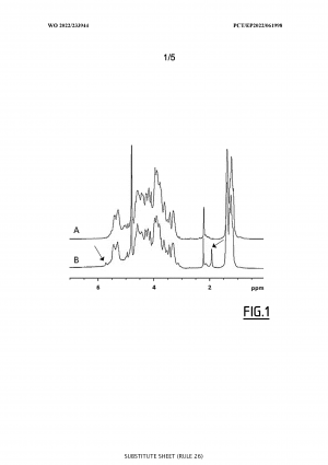
Membrane nanocomposite à film mince à base d’une structure organique métallique encapsulée dans un liquide ionique pour la séparation d’ions métalliques IRAMIS, NIMBE, LICSEN 28 décembre 2023
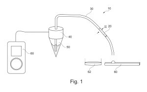
Procédé de détection magnétique d’objets biologiques microscopiques et dispositifs associés IRAMIS, SPEC, LNO 28 décembre 2023
Utilisation de particules de dioxyde de titane portant un métal ou un oxyde de métal pour l’obtention d’alcènes par photocatalyse IRAMIS, NIMBE, LEDNA 7 décembre 2023
Procédé de fabrication d’une architecture amorphe de type micro-treillis formé de micro-poutres reliées entre elles par des nœuds IRAMIS, SPEC, SPHYNX 21 septembre 2023
Procédé d’extraction sur phase solide à l’aide d’un monolithe poreux IRAMIS, NIMBE, LEDNA 7 septembre 2023
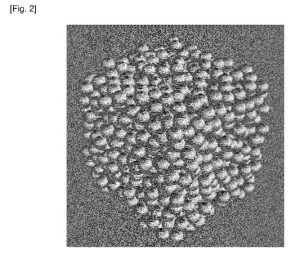
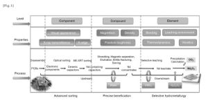
Procédé de recyclage de néodyme à partir de cartes de circuits imprimés usagées IRAMIS, NIMBE, LICSEN 24 août 2023
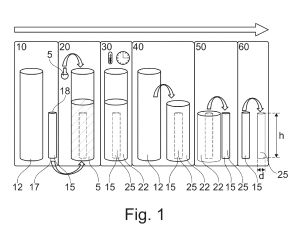
Procédé de fabrication d’un monolithe poreux par un procédé sol-gel IRAMIS, NIMBE, LEDNA 29 juin 2023
Procédé et système pour la mesure de concentrations relatives de matériaux d’un mélange par mesure de susceptibilité magnétique dynamique (AC) IRAMIS, SPEC, LNO 29 juin 2023
Procédé et appareil de génération d’impulsions électromagnétiques ultrabrèves isolées IRAMIS, LIDYL, PHI 29 juin 2023
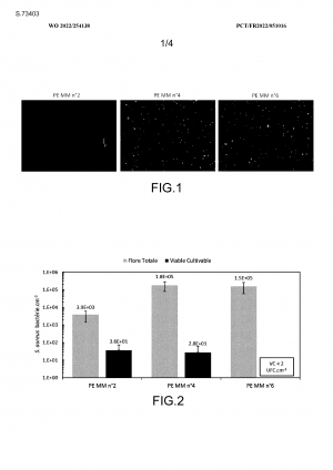
Utilisation de polymères d’aluminosilicate à titre d’ingrédient actif contre les microorganismes phytopathogènes IRAMIS, NIMBE, LIONS 26 juin 2023
Procédé de préparation d’anhydride cyclique à partir d’un acide carboxylique insaturé IRAMIS, NIMBE, LCMCE 19 mai 2023
Mélange-maître à activité bactériostatique ou bactéricide, son procédé de préparation et ses utilisations IRAMIS, NIMBE, LICSEN 8 décembre 2022