L’invention concerne un procédé de réalisation d’une puce (40) de dépôt de films minces, comportant :
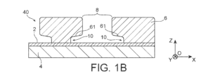
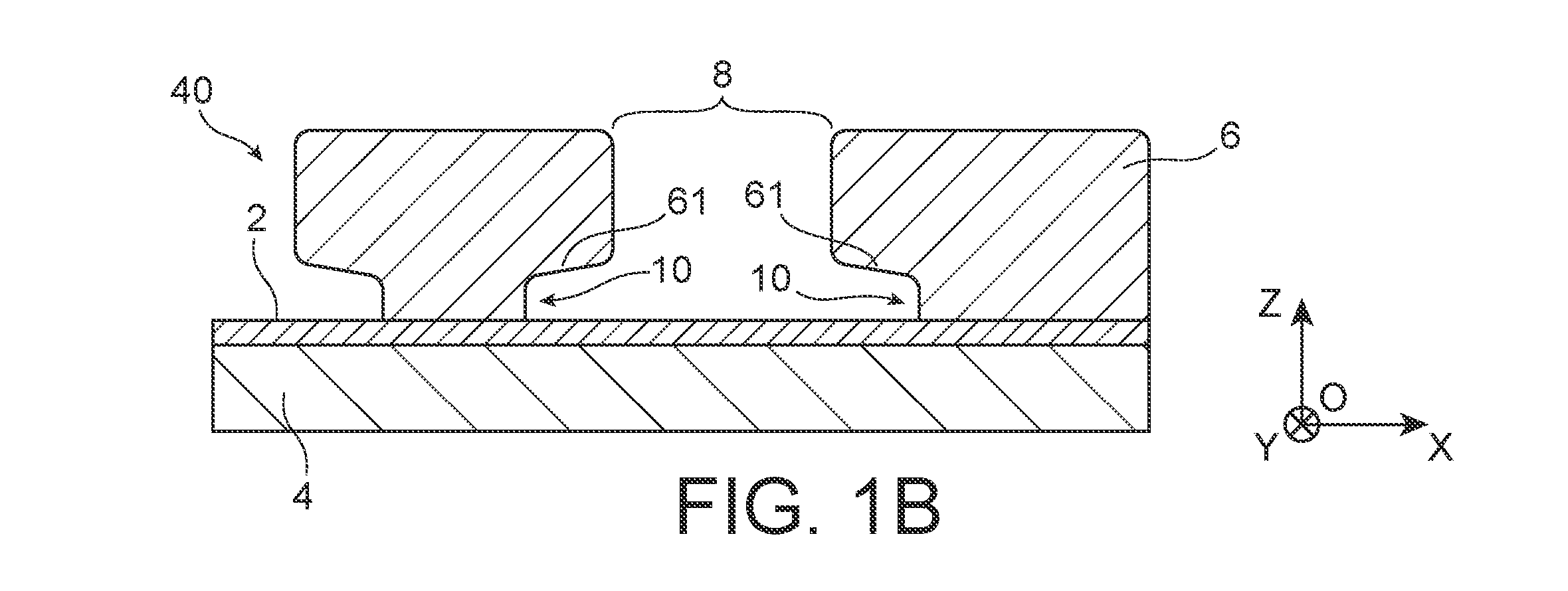
a) – la formation, sur un substrat (4) en un matériau isolant ou semi-conducteur, d’une pluralité d’électrodes de mesure (2), chaque électrode ayant une partie centrale et des bords inclinés vers la surface du substrat (4);
b) – la formation d’un masque (6) de dépôt, définissant une fenêtre (8) de dépôt, ce masque comportant des échancrures (10) au voisinage du substrat et de ladite fenêtre.
Contact CEA-Iramis : Hélène Le Sueur (SPEC/GQ),
Method for measuring the resistance and capacitance of thin films during deposition
The invention relates to a method for producing a thin film deposition chip (40), comprising:
a) – forming, on a substrate (4) made of an insulating or semiconductor material, a plurality of measurement electrodes (2), each electrode having a central portion and edges inclined towards the surface of the substrate (4);
b) – forming a deposition mask (6), defining a deposition window (8), said mask having indentations (10) in the vicinity of the substrate and of the window.
Contact CEA-Iramis: Hélène Le Sueur (SPEC/GQ),