Scanning Tunneling Microscopy (STM) is a technique developed in the laboratories of IBM in Zurich by Gerd Binning and Heinrich Rohrer (Nobel Prize of Physics in 1986).
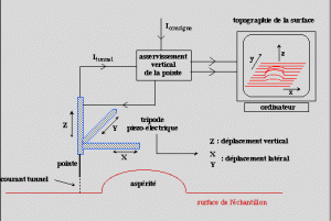
This technique is based on a known physical phenomenon since the origins of quantum mechanics, the tunnel effect. A STM consists of two electrodes of reasonable conductivity of which one has the shape of a tip and the other is the surface of the studied film. The tip-sample distance is about a few angströms. If a biasing is applied between the tip and surface, the electrons have a nonnull probability to pass from one electrode to the other and a tunnel current thus will be born. The principle of the experiment consists in moving the point above the film surface (using piezoelectric ceramics) by maintaining the tunnel current constant by a servo system. Thus the tip-sample distance remains constant and the recording of vertical displacements of the tip then reproduces accurately the topography of surface. If the tip is sufficiently fine (few angströms), the relief observed can have the atomic resolution. The STM experiment can also work in spectroscopic (Scanning Tunneling Spectroscopy or STS) mode. In this case, the tip is maintained fixed compared to the surface of the sample to a given position. The servo-control is opened and a V(t) voltage slope is applied between the tip and the surface of the sample. For each applied voltage the tunnel current is measured and the study of the current-voltage characteristics give access the local electronic density of states on the surface.

Instrumentation
STM measurements are generally carried out in an ultra-high vacuum chamber in order to avoid a possible contamination of surface by the residual atmosphere. The sketch of a STM is represented below. A STM microscope include the following elements:
- a conductive tip (tungsten, platinum, gold …)
The tip plays the role of local probe of the tunnel current and constitutes a measure of the electronic density. This one, positioned with a few angströms, is carried to a potential positive (or negative) of a few volts compared to the the sample surface in order to probe the full (or empty) states of the sample. The lateral resolution of the STM image is determined by the tip diameter. To obtain an atomic resolution, it is necessary that the tip is finished by an atom. The preparation of the tip is a crucial element for obtaining images of high quality and various methods were developed: vaporation by heating, electrochemical deposition, …

- a whole of three piezoelectric ceramics allowing the displacement of the tip
Displacements of the tip in the three directions (X, Y, Z) are controlled by piezoelectric quartz. A voltage is applied to each piezoelectric ceramics thus causing a contraction or a dilation of this one according to the polarity. Displacement in directions X and Y makes it possible to scan the surface of the sample whereas according to direction Z, a loop of control obliges the point to move normally on the surface to maintain a tunnel current constant. Displacements are done with a precision being able to go from a fraction of angström to some micrometers.
- an acquisition and data analysis electronic system
- an antivibration device
Several systems can be used to damp out the high frequency vibrations (anti-vibratory metal plates, systems with spring combined with absorbing materials …).


