
Guolei Tang, Zhang Xinfeng, Yang Shihe, Vincent Derycke and Jean-Jacques Benattar
(
Recently Jean-Jacques Benattar and his co-workers at SPEC, CEA-Saclay have developed a simple and original technique to produce surfactant films containing nano-objects such as nanoparticles, nanowires etc. and to transfer such films onto solid substrates [1]. As described in their article appearing in June issue of SMALL, this technique has now been applied to transfer thin films of monolayer, highly-oriented and dense single wall carbon nanotubes (SWNT) onto silicon substrates. The successful creation of aligned and dense SWNT networks is a technological breakthrough toward the commercialization of electronic components based on carbon nanotubes. JJ Benattar explains:
The combination of excellent mechanical and electrical properties of single wall carbon nanotubes (SWNTs) could lead to numerous applications in a wide spectrum of fields spanning from flexible electronics, biosensors to solar cells and much more. At present; however, the effort to use SWNTs as functional elements in the electronic devices is hindered by their low output current. Moreover, the integration of SWNTs into electronic circuits requires solving the delicate synthesis problems and precise positioning of a large number of electrically homogeneous nanotubes. The use of thin films made out of dense networks of horizontally aligned nanotubes would avoid these obstacles while preserving the valuable properties of individual nanotubes. If achieved, such films will have a great potential for low-cost, high-performance electronics that are compatible with a wide variety of substrates, including flexible organic materials.
A variety of techniques on nanotube depositions and localized growth have been reported in literature to date (Evaporation, Langmuir-Blodgett etc.). The most common is the direct growth of nanotubes on a substrate by CVD (Chemical Vapor Deposition) method. However, this technique cannot easily accommodate simultaneously both a high density and a good alignment of nanotubes, and it is not compatible with many types of substrates due to the high temperature at which the nanotubes are grown (typically 800-900 ° C). In addition, the CVD technique invariably produces an admixture of metallic and semiconducting nanotubes. Various low temperature deposition techniques have also been investigated, such as spin-coating and the Langmuir-Blodgett transfer to name a few. It is still unclear; however, whether these methods can produce large areas of dense, organized nanotube films.
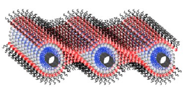
Previously, we have developed a simple, original method to transfer surfactant films containing monolayer nano-objects onto solid substrates (“Process for deposition of nanoscale thin film on a substrate”®)[1]. In the present work [2], we have achieved another milestone; namely, the confinement of single wall carbon nanotubes in a film and its transfer onto a solid surface. First, the surfactant (sodium dodecyl benzene sulfonate, SDBS) is used to disperse SWNTs in aqueous solution (Figure 1a). Subsequently, the surfactant bubbles made out of thin films containing SWNT are formed under controlled humidity. Figure 1c shows that the draining of water from such a bubble leads to the formation of a ‘black’ film that is too thin to reflect light. The water drainage leads to the confinement and simultaneously, the alignment of nanotubes. A hydrophobic solid substrate is then placed in contact with the bubble to make the transfer (See Figure 1d).
|
Figure 1a): SDBS surfactant coated SWNT. b): Schematic view of a deposited film consiting of monolayer SWNT. c): Photographic image of Black Film in making. d): Film deposition on to a substrate approaching from the top.
|
Figure 2: AFM image of aligned SWNT film (central zone)
|
The deposited film consists of a monolayer SWNTs locked in a SDBS bilayer (Fig. 1b). AFM (Atomic Force Microscopy) images of the deposited film were taken from different locations on the substrate. A high density SWNT film is obtained over the entire deposition area. In the centre of the film, corresponding to the top of the bubble, carbon nanotubes are randomly oriented. But away from the central zone, SWNTs are very well-aligned (Figure 2). This marked difference in alignment between the centre and the outer zones is induced by the water drainage from the bubble before deposition. The AFM image analysis shows an excellent degree of alignment; i.e., ~ 80% of SWNTs lie within a 15° spread, and a uniform film thickness that is compatible with the height of monolayer nanotubes.
In summary, we have successfully applied the bubble wall confinement of nano-objects and its deposition method to the formation of thin films with dense, well-aligned carbon nanotubes. We have also demonstrated the compatibility of this method with flexible organic substrates such as. One major advantage of our technique is its applicability to all types of nanotubes, especially those pre-sorted by chirality or by electrical property. The technique can also be extended to include other types of nano-objects where organized film making is of an important issue.
To see Black Film making in action, click
[1]
– a) Adhesion of a Free-Standing Newton Black Film onto a Solid Substrate, Benattar J.J., Nedyalkov M., Lee F.K., Tsui O.K.C. Angew. Chem. Int. Ed. 45 4186-4188
– b) European patent “Procédé de dépôt de film mince nanométrique sur un substrat”, J.J Benattar,
Patent pending: No 06 04297, 15 may 2006, Commissariat à l'Energie Atomique.
[2] Une nouvelle méthode pour la formation de monocouches très dense de nanotubes de carbone alignés. Tang Guolei, Zhang Xinfeng, Yang Shihe, Derycke Vincent et Jean-Jacques Benattar, SMALL 6, 1488-1491 (2010).