Invité par Yannick DAPPE.
Abstract :
Graphene nanoribbons (GNR) are suitable candidates for sensor devices. Their dimensions (one-atom thickness and widths of tens of nanometers or less) make it difficult to experimentally correlate their electrical properties with changes in their width, edge structure or defect concentration. In this context, we discuss two examples in which GNR-based devices were characterized and also modified within a transmission electron microscope (TEM) with the electron beam while an electrical bias was applied.
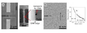
In the first example, we describe how to use the converged electron beam of a TEM to fabricate GNR-nanopore devices, which are promising candidates for next-generation DNA sequencing.1 Such devic-es normally comprise a 2-10 nm diameter pore formed with the beam at the edge or in the center of a 50-100 nm-wide GNR on a 50 nm-thick silicon nitride membrane. We discuss the changes on GNR conductance when such devices are irradiated with a 200 keV beam and the differences between irra-diating with a homogenous (TEM mode) versus a scanned condensed beam (STEM mode). By mini-mizing the electron dose at 200 kV in STEM mode we were able to prevent electron beam-induced damage and make nanopores in highly conducting GNR. The resulting devices, with unchanged re-sistances after nanopore formation, can sustain micro ampere currents at low voltages (∼ 50 mV) in buffered electrolyte solution and exhibit high sensitivity, with a large relative change of resistance upon changes of gate voltage, similar to pristine GNR without nanopores (see Figure A).

(A) GNR-nanopore device for DNA translocation measurements. (B). High resolution TEM image of electrically biased sub-10 nm GNR with lattice information; GNR resistance as a function of width.
In the second example, we describe how to use the condensed beam of a TEM with corrected spheri-cal-aberrations to sputter carbon atoms from predefined areas in electrically-connected free-standing graphene sheets to obtain GNR with sub-10 nm widths.2 This approach allows us to correlate the lat-tice and edge structure of sub-10 nm wide GNR with their electrical properties (see Figure B). In this way we were able to measure sustaining currents in excess of 1.5 μA per carbon bond across a 5 atom-wide ribbon.
1. Toward sensitive graphene nanorib-bon–nanopore devices by preventing electron beam-induced damage
Puster, M.; Rodríguez-Manzo, J. A.; Balan, A.; Drndić, M. . ACS Nano 7 (2013) 11283.
Qi, Zhengqing J.; Rodríguez-Manzo, J. A.; Botello-Méndez, A. R.; et al. Nano Letters 14 (8) (2014) 4238.
Department of Physics and Astronomy, University of Pennsylvania, USA


