
SPEC has progressively equipped itself with a nanofabrication lab, where research groups can produce their devices. This CEA facility, awarded the label “Centrale de Proximité” in 2004 by the French Ministry of Higher Education and Research, is also supported by the CNRS, the Ile de France Region and the ANR (Agence Nationale de la Recherche).


SPEC’s Nanofabrication Facility has been awarded the label “Centrale de Proximité” by the Renatech network.
Access is free for those who have received the necessary training. External users may have access if they are actively collaborating with at least one SPEC team. When an external project is submitted, it is presented to the steering committee, which assesses its feasibility with existing resources. For such a project to be accepted, it is essential that a SPEC group takes on the task of supervising and assisting the users involved in the project.
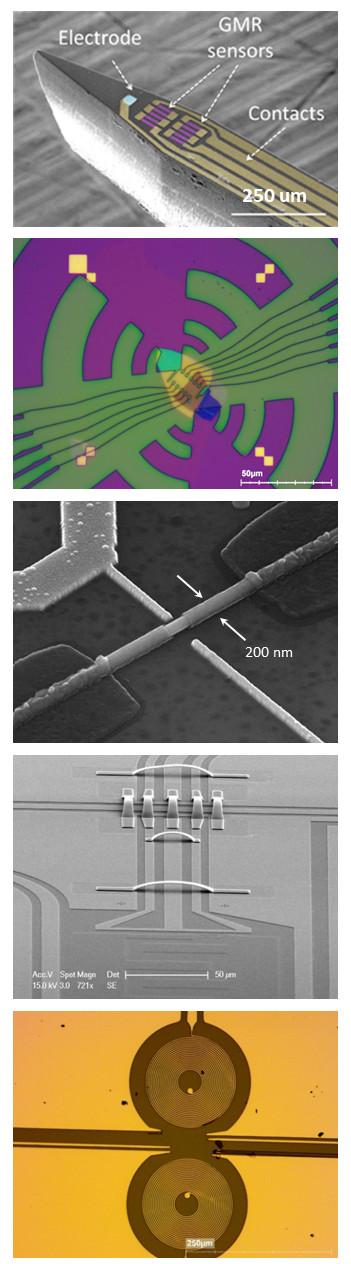
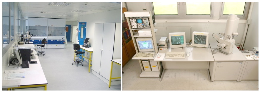
The facility consists of a class 10000 clean room built in 2006 (115 m²) and a class 100000 “grey” room (50 m²). The first one is equipped for optical lithography, sample preparation (wet and dry chemical etching) and characterization. The second houses thin-film deposition equipments (2 evaporators, 2 sputterers) and an electron beam lithography research tool.
Other equipment are located in conventional laboratories (120 m²), where dust levels are not controlled: SEM electron lithography, thin-film deposition equipment, characterization equipment.
Two permanent engineers and a technician are in charge of the workshop’s operation and maintenance.
Some 100 users are registered for access, and around 40 work there regularly.
Contact: Pierre-Francois ORFILA