

Molecular Electronics is a field of research that aims at designing new electronic devices based on molecules. Unfortunately, lack of stability of molecular junctions induces a lack of reproducibility in the measurement process which prevents from a large scale utilization, in particular at the industrial level. A potential approach to overcome this difficulty lies in performing in operando characterizations, in order to get a better understanding of molecular devices and to improve their reliability.
This is what has been achieved through the collaborative work of different research teams from IMDEA-Nanociencia, Universidad Autonoma and Universidad Complutense in Madrid, University of Barcelona, ALBA Synchrotron and Centro de Astrobiologia in Torrejon de Ardoz, in Spain, and SPEC at University Paris-Saclay. These researchers have designed and realized a multifunctional hybrid molecular graphene field effect transistors which enables in operando spectroscopy.
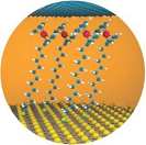

Figure :
- Design of the fabricated device where the different layers are artificially separated for clarity. Fabrication is sup- ported on a Si++/SiO2 (290 nm) wafer. Starting with a photolithography step for the fabrication of the Cr/Au (6/60 nm) electrodes, followed by 8 nm ALD growth HfO2 to insulate the electrodes and opening of micropores in the HfO2 by dry etching (HF). The micropores areas allow controlling the surface area of the electrical contact. After thiol adsorption and Gr transfer, a third lithography step to pattern the Gr completes the fabrication process.
- Cross-section of the device with electrical connections including: back gate voltage (VBG), drain source voltage (VDS) and drain source current (IDS)
- Molecular detail. Sulfur and gold are linked by a covalent bond, upwards 11 sp3 carbon atoms and on top the Fc group connecting a single Gr layer by π-π interactions. Drawing is not to scale.
- Evolution of the X-ray absorption spectra from a 5 μm pore where the FcC11SH is placed and connected with graphene on top at different source to drain voltages, measurements from t = 0 to t = 5 are performed every 20 minutes by changing the VDS from 0 to 1, 2, 0, −1 and −2 V. Vertical dashed lines are incorporated for guide the eye at 708.8 and 710 eV that corresponds to the presence of Fe2+ and Fe3+ respectively.
- Source-drain photo- conductance is displayed versus the gate voltage at ambient conditions during pulsed light illumination (21.5 mW LED). Electrons excited by the light in the Fc group do not affect the photoconducatance if VBG < VDP (VDP, is the back gate voltage at the conductance minimum). However, electrons are injected to the Gr conduction band when VBG > VDP giving rise to light photodetection.
As represented in the Figure, the device is composed of a gold layer deposited on SiO2, and a graphene monolayer, separated by an insulating HfO2 layer. In between, a self-assembled monolayer of SC11Fc has been deposited which makes the molecular bridge between gold and graphene electrodes. This particular configuration, free from ionic liquid, allows the implementation of optoelectronic logic gates in order to improve the device reproducibility and scalability in modern electronics. Indeed, on the one hand graphene enables redox electron transfer, avoiding however molecular degradation, and therefore permits in operando spectroscopy. As such, the device has been fully characterized by electrochemical, AFM and CAFM, XPS, UPS, XAS, Raman and optoelectrical measurements. On the other hand, molecular electrode decoration shifts the graphene Dirac point to neutrality and derives photocurrent.
Experimental results are supported by Density Functional Theory (DFT) calculations, which allow to determine the electronic structure and transport of the molecular junction. In particular, it shows that the junction exhibits very low rectification, which is due to the symmetry breaking induced by the use of a graphene electrode.
This innovative transistor configuration may find application in ultrasensitive photodetectors and new optical circuits.
Référence :
Hybrid molecular graphene transistor as an operando and optoelectronic platform
J. Trasobares, J. C. Martín-Romano, M. W. Khaliq, S. Ruiz-Gómez, M. Foerster, M. Á. Niño, P. Pedraz, Y. J. Dappe, M. Calero de Ory, J. García-Pérez, M. Acebrón, M. Rodríguez Osorio, M. T. Magaz, A. Gomez, R. Miranda & D. Granados, Nature Communication 14 (2023) 1381.
Contact : Yannick Dappe, SPEC/GMT
Collaboration :
- IMDEA-Nanociencia, Cantoblanco, Madrid, 28049, Spain
- Department of Biodiversity, Ecology and Evolution (Biomathematics), Universidad Complutense de Madrid, Madrid, 28040, Spain
- ALBA Synchrotron, Carrer de la llum 2-26, Cerdanyola del Valles, 08290, Spain
- Department of Condensed Matter Physics, University of Barcelona, Barcelona, Spain
- Centro de Astrobiología (CSIC-INTA), Torrejón de Ardoz, 28850, Spain
- Université Paris‐Saclay, UMR SPEC CEA-CNRS, Gif-sur-Yvette, 91191, France
- Dpto. de Física de la Materia Condensada, Universidad Autónoma de Madrid, Cantoblanco, Spain