

Graphene is a very promising material for a wide range of applications in Nanoelectronics. Unfortunately, it presents a metallic character, which implies the need to look for alternative strategies in order to design and fabricate elementary electronic devices like diodes or transistors. This aspect constitutes a severe limitation in the field of numeric electronic or future telecommunications. A possible way to overcome this limitation is to consider new 2D materials in order to combine them with graphene eventually, in the design of future nanoelectronic devices. In this respect, phosphorene, a 2D material composed of one or several atomic layers of black phosphorous, offers a new opportunity to tackle this challenge. Indeed, phosphorene is a 2D semiconductor with very interesting properties compared to the ones of graphene. In particular, phosphorene combines in the meantime a direct bandgap, which is tunable as a function of the number of layers, and a high value of charge mobility.
Until now, similarly to numerous 2D materials, phosphorene has mainly been obtained through exfoliation process. However, in order to obtain well-controlled phosphorene layers, procedures commonly used in industry like molecular beam epitaxy (MBE) and chemical vapour deposition (CVD) must be used to explore a large range of growing conditions and therefore to develop protocols adapted to the fabrication of new electronic devices.
In this context, three teams from Université Paris Saclay, namely ISMO-CNRS, TEMPO-Synchrotron SOLEIL and SPEC (CEA-CNRS), in collaboration with a group from Central Florida University, have achieved for the first time the synthesis of phosphorene chains on silver using MBE.
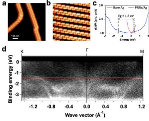
In this work, the researchers have evaporated phosphorous atoms under ultra-high vacuum on a (111) oriented silver crystal. The combination of tunnelling microscopy and spectroscopy (STM-STS), low energy electron diffraction (LEED), photoelectron spectroscopy (PES) and angle resolved photoemission spectroscopy (ARPES) has allowed identifying the atomic and electronic structures of phosphorene chains. These phosphorene chains exhibit an armchair shape and present a semiconductor character with an intrinsic bandgap of 1.8 eV (Figure 1).

Density Functional Theory (DFT) calculations have allowed to validate the obtained atomic structures and to determine their corresponding electronic properties, confirming the semiconductor character of the obtained chains. The latter is attributed to the passivation of phosphorous atoms on the silver surface (Figure 2a, 2b). In addition, the simulated STM image is in very good agreement with the experimental one (Figure 2c).
These findings open very promising perspectives for the potential integration of networks of phosphorene wires as 2D material in electronic devices.

Reference:
Flat epitaxial quasi-1D Phosphorene chains, Wei Zhang, Hanna Enriquez, Yongfeng Tong, Andrew J. Mayne, Azzedine Bendounan, Alex Smogunov, Yannick J. Dappe, Abdelkader Kara, Gérald Dujardin, and Hamid Oughaddou, Nature Communications 12, 5160 (2021)
Contact:
Yannick Dappe (CNRS), Modeling and Theory Group (SPEC/GMT), CEA Saclay
Hamid Oughaddou, Institut des Sciences Moléculaires d'Orsay (ISMO), Université Paris Saclay
Collaboration :
- Service de Physique de l’Etat Condensé (SPEC), UMR 3680 CEA-CNRS, Université Paris-Saclay
- Institut des Sciences Moléculaires d’Orsay (ISMO), CNRS, Université Paris-Saclay
- TEMPO Beamline, Synchrotron SOLEIL, Gif-sur-Yvette
- Department of Physics, University of Central Florida, Orlando
Communiqué CNRS: https://www.iledefrance-gif.cnrs.fr/fr/cnrsinfo/des-atomes-de-phosphore-deposes-en-chaine