
Ludovic Douillard et Fabrice Charra, DRECAM/SPCSI/Groupe Nanophotonique
A reduction of the size of a metallic object results in significant changes in its physical properties and in particular its response to an optical excitation. Noticeably, for objects of sizes significantly smaller than the incident wavelength, resonances in the absorption spectrum appear. These, called plasmon resonance, correspond to a process of collective oscillation of the electrons, as described by Mie at the beginning of the 20th century [Mie 1908]. In the case of noble metals, these resonances are in the visible spectrum, a phenomenon known since ancient times for obtaining coloured glasses by inclusion of metallic particles.
Today, the development of nanotechnology involves a great interest in such phenomena, now grouped together in a new topic named plasmonic. Beyond its fundamental aspects, the subject has a wide range of technological applications, from the design of optical components (polarizers, waveguides…) to genetic analysis (biochemical… detector).
The associated physics involve the coupling between the conduction electrons and the electromagnetic field associated with the incident radiation. For a size lower than the wavelength of the radiation, the electrons are confined within a single object and the electromagnetic field is seen as uniform in space and time. The oscillating nature of the excitation results in a collective and coherent movement of the electrons: the plasmon resonance. The next step is the design of assemblages of such objects, which plasmon modes, under optical excitation, are coupled according to the chosen geometry.

The usual experimental method to investigate the phenomena is mainly the scanning near-field optical microscopy (SNOM), where the electric field is measured using a local probe (fiber optic…). However the high spatial resolution is counterweighed by the significant disturbance induced by the presence of the probe.
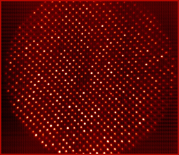
In an effort to overcome these disruptions inherent to the near-field microscopy, we show that the photoelectron microscope PEEM (Photo-Electron Emission Microscopy) opens up very interesting perspectives by its ability to map the two-dimensional distribution of photoelectrons emitted from a surface. The principle of optics imaging is electronic and no probe is used close to the system under study. The distribution of emitted electrons corresponds to a process of non-radiative relaxation of the excited surface plasmon modes. The experimental results compare favorably to those obtained by SNOM (with 50 nm resolution) and the experimental degrees of freedom allow access to a wide range of geometries of excitation (grazing or normal incidence). The test of photoelectron microscopy as a tool for characterization of the near-field optics is ongoing in the context of the study of individual items or assemblies and geometries.
[MIE 1908] G. Mie, Ann. Phys. (Leipzig) 25 (1908) 377.
Contact: Ludovic Douillard et Fabrice Charra