Contact : Ludovic DOUILLARD
Ludovic Douillard1, Fabrice Charra1, Zbigniew Korczak1, Renaud Bachelot2, Sergei Kostcheev2, Gilles Lerondel2, Pierre-Michel Adam2 and Pascal Royer2
1CEA-Saclay, DSM/IRAMIS/SPCSI Service de Physique et Chimie des Surfaces et Interfaces,
2Laboratoire de Nanotechnologie et d’Instrumentation Optique, ICD CNRS FRE 2848, Université de Technologie de Troyes
Since the very beginning of electronics, technological efforts have been continued for designing circuits with higher integration and for handling information at higher frequencies. Thus, electrical and electronic devices are becoming more miniaturized, more complex (like the micro-processors in our computers). They remain however limited to frequencies of the order of one gigahertz (1 GHz = 109 Hz, 30-300 GHz in the lab). The optical frequencies are one million times higher (1015 Hz), but space limitations imposed by the wavelength of light (measured in tenths of micron) prevent the very high integration of optic components.
An intermediate solution can be obtained by converting the optical signal into plasmons (or electronic charge oscillations with respect to the crystalline network of atomic nuclei), providing this is performed at the surface of a nanometer sized conductor.
Electro-magnetic field and plasmons can be strongly coupled: the incident light excites the plasmon and a plasmon, by an antenna effect radiates. If for a thick object, the wavelength of the plasmon is of the same order as that of the optical wave, it is not the same if the transverse dimension of the object falls below the nanometric penetration depth of the incident wave (typically <30 nanometers). A plasmon is then created on each of the interfaces, and by interference two separate plasmon modes result. One of these modes (called slow plasmon) oscillates at the frequency of the light wave but with a much smaller wavelength (reduction sometimes better than a factor of 10!)
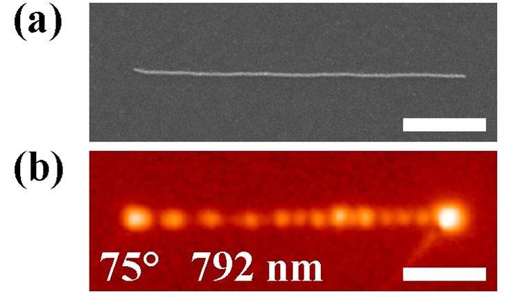
These principles were known, but remain to be observed. It is possible to visualize and explore plasmons excited by light observing their non-radiative de-excitation in the form of electron emission. The idea was then to use a PEEM (photoemission electron microscope), which allows getting high resolution images of the electron emitting areas. The first figure above shows the emission from a gold wire. The intensity modulations result from the interferences between the created slow plasmon and the excitation light wave.
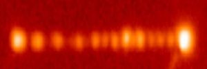
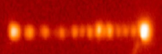
The second image shows the electronic emission from a network of Au nanorods of increasing lengths (between 50 nm and 1 μm). Only antennas resonant with the incident light are excited and emit electrons. These observations can be reproduced by a simple analytical resonator model.
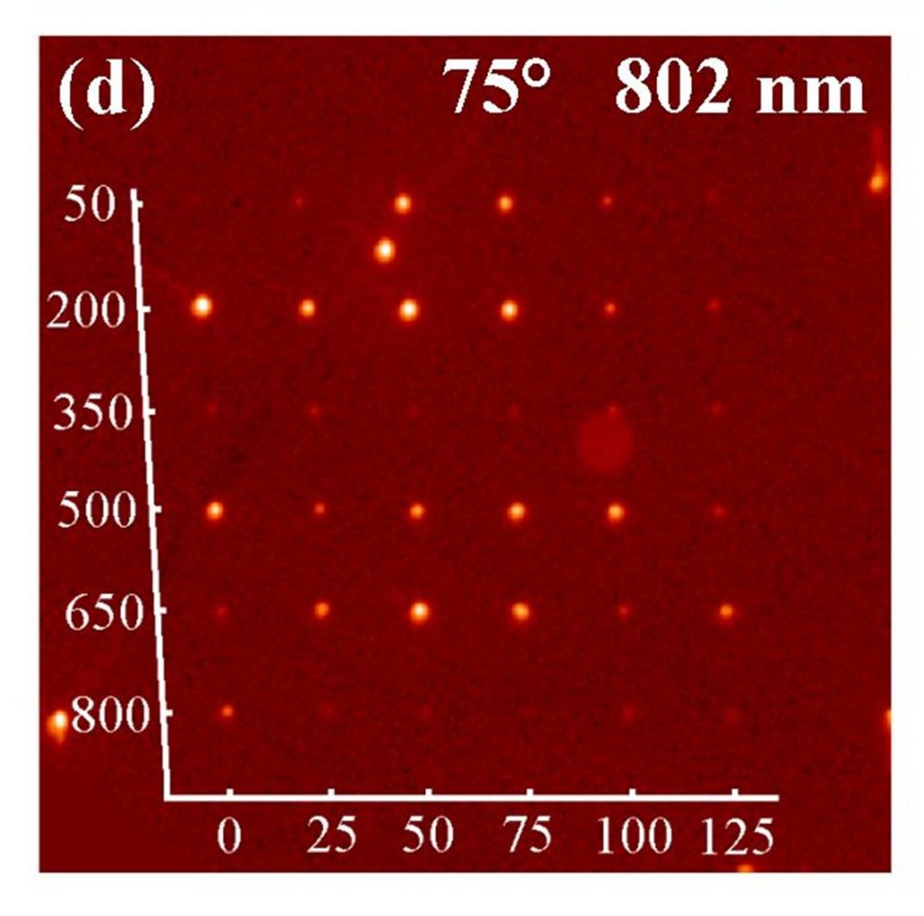
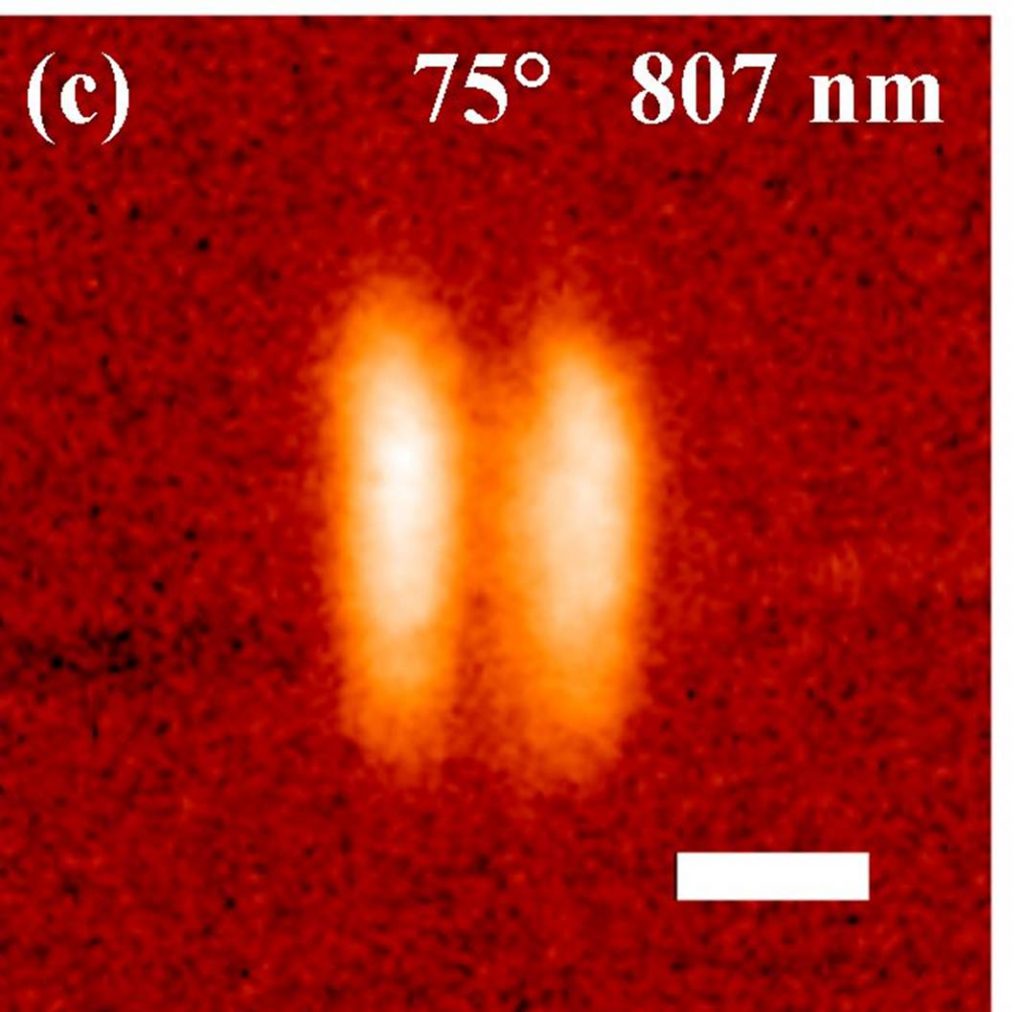
The last image at very high resolution shows the plasmon mode (λ/2 dipolar mode) of a 100 nm long nanorod excited by a light radiation of wavelength 807 nm. The excitation wavelength is reduced by a factor 3.
These experiments show that, by converting the information of an optical signal into a slow plasmon, it is possible to conciliate high frequencies and low spatial dimensions. The basic requirement for the wavelength reduction is to design structures with one transverse dimension typically less than 30 nm (cross the “nano” wall!). The road is still long before the realization of complex devices, but experiments conducted in the laboratory of SPCSI show the reality of the principle and its feasibility
L. Douillard, F. Charra, Z. Korczak, R. Bachelot, S. Kostcheev, G. Lerondel, P.-M. Adam, and P. Royer, à Nano Letters 8(3) (2008) 935.
See also:
- The CEA-Université de Troyes press release.
- In “Le Monde Informatique” : Observer la compression de la lumière pour une gravure plus fine ©
- Bulletin de l’Agence pour la Diffusion de l’Information Technologique (ADIT) : La compression de la lumière observée en direct
- Fait marquant 2006 : Optics of nano-objects – Visulisation of plasmon excitations by photo-emission electron microscopy (PEEM)