

Storing information even when the power is switched off is one of the key challenges driving the development of new memory technologies. Ferroelectric memories are among the promising approaches being explored, but the materials they rely on can be altered by the high temperatures involved in manufacturing. Researchers from the Condensed Matter Physics Laboratory (SPEC, CEA/CNRS/Université Paris-Saclay), part of IRAMIS, have worked with STMicroelectronics to investigate what happens at the interface between two layers of these devices during fabrication. Their findings reveal that temperature promotes chemical reactions and the accumulation of defects near this interface, providing valuable insight into factors that may affect the reliability of future non-volatile memory devices.
Ferroelectric memories rely on a distinctive property: their ability to retain an electrical polarization state even after an applied voltage is removed. This state can be used to store information. Hafnium oxide is of particular interest because it can exhibit ferroelectric properties in layers just a few nanometers thick, making it compatible with current semiconductor manufacturing processes. However, these processes require materials to undergo an activation anneal of dopants in the silicon at high temperature. Such heat treatments can alter their structure and chemical composition, particularly at the interfaces between different layers. One concern is the formation of oxygen vacancies, produced at or near the gate/ferroelectric interface, which can influence ferroelectric properties and device reliability.
To investigate how these defects form and are distributed, the researchers examined multilayer structures representative of those used in ferroelectric field-effect transistors (FeFETs). These structures include a thin layer of silicon-doped hafnium oxide covered by a titanium nitride metal gate gate. Two samples, fabricated at STMicroelectronics using industrial manufacturing processes, underwent 30-second activation annealing at 750 and 1,000 °C, respectively. The main challenge was to investigate the interface buried beneath the metal electrode. To overcome this, the team used X-ray photoelectron spectroscopy (XPS), a technique that provides information about chemical elements and their local environments by analyzing electrons emitted when a material is exposed to X-rays. By carefully thinning the electrode without damaging the gate/ferroelectric interface and varying the measurement angle, the researchers were able to probe different depths of the HfO2 beneath the gate. Transmission electron microscopy provided complementary observations.
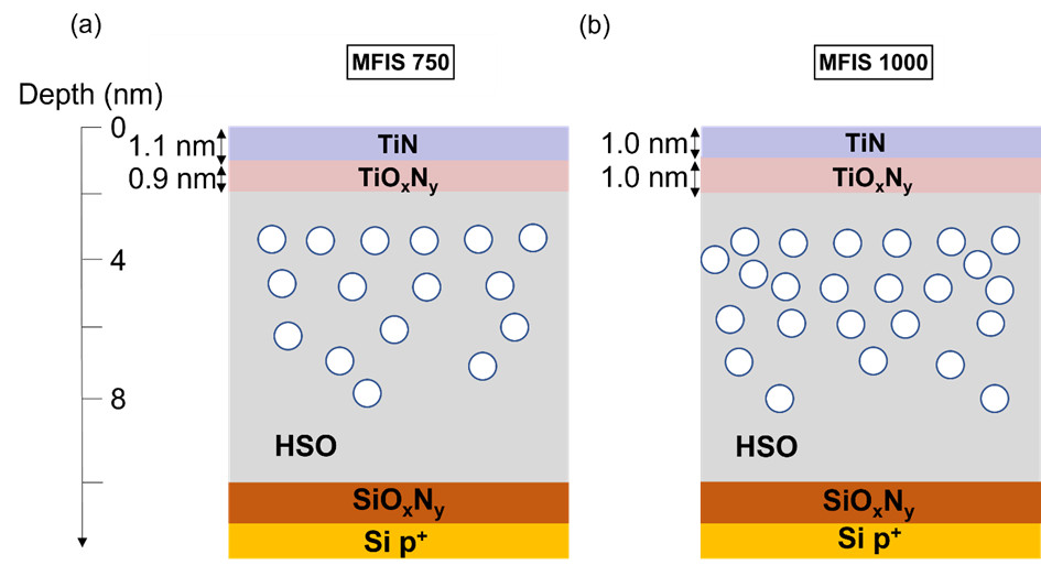
Figure: Schematic of the main result of the study. For the two stacks, annealed at 750°C (MFIS750) and 1000°C (MFIS1000), an oxygen vacancy (white circles) concentration profile is observed. However, the absolute concentration is significantly higher after annealing at 1000°C, much closer to the usual industrial Front End process conditions.
The results reveal a chemical transformation where the two layers meet. Part of the titanium nitride is converted into titanium oxynitride, forming an interfacial region approximately one nanometer thick. This transformation reflects a process known as oxygen scavenging, in which the metal electrode draws oxygen from the adjacent ferroelectric material. The measurements also show that signatures associated with oxygen vacancies are stronger near this interface than deeper within the film. This distribution is observed in both samples but is consistently more pronounced following annealing at 1,000 °C. The higher temperature therefore leads to a greater concentration of vacancies throughout the region examined, while the overall shape of their depth distribution remains largely unchanged. These observations demonstrate how manufacturing conditions influence the chemistry of this buried interface.
The researchers also identified changes in the material’s electronic properties. After annealing at 1,000 °C, the hafnium photoelectron spectra exhibit a binding-energy shift of approximately 0.20–0.25 eV, consistent with a change in the local electrostatic potential associated with the higher concentration of charged defects. Other effects, including chemical changes at the interface, may also contribute to this shift. Electron microscopy images further show that the overall multilayer structure remains intact, although the interface between the electrode and the ferroelectric layer appears more diffuse than in the bulk of the film. These observations support the interpretation that chemical reactions are primarily concentrated near the metal electrode. One important limitation remains: oxygen vacancy concentrations are inferred indirectly from the hafnium spectra, which may also contain contributions from other chemical environments, for example, Hf-N. Nevertheless, the comparative trends observed at the two annealing temperatures remain consistent.
For a new memory technology to eventually find its way into everyday electronic devices, being able to store information is only part of the challenge. It must also be reliable and compatible with industrial manufacturing processes. This is where the findings are particularly relevant: they show how a high-temperature fabrication step can alter the chemistry and electronic properties of materials at the nanometer scale. By identifying these changes, the researchers provide a clearer understanding of how manufacturing conditions can influence the factors that determine the reliability of ferroelectric memories. Although the study does not demonstrate improved device performance, it adds to the knowledge needed to develop reliable non-volatile memories that could one day be integrated into future electronic devices.
Reference
T. Iung, L. Pérez Ramírez, C. Lubin, I. Bottala-Gambetta, R. Beneyton, D. Cooper, M. Gros-Jean and N. Barrett. “X-ray photoelectron spectroscopy study of gate/ferroelectric interface chemistry in metal–ferroelectric–insulator–semiconductor stacks.” Journal of Applied Physics, 140, 104102 (2026).
Collaboration
Contact
Nicholas Barrett, Researcher at LENSIS group, SPEC (UMR CEA-CNRS).