Microscopie à effet tunnel par émission de photons perfectionnée
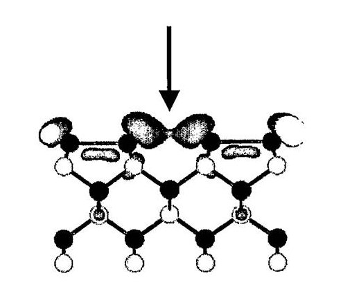
La présente invention concerne un substrat semi-conducteur à gap indirect, supérieur au gap du silicium, préférentiellement supérieur à 1,5 eV, son utilisation pour imager un échantillon par microscopie à effet tunnel en émission de photons, ainsi qu’un procédé d’imagerie à effet tunnel en émission de photons utilisant un tel substrat semi-conducteur à gap indirect. Avantageusement, le substrat semi-conducteur à gap indirect est le carbure de silicium. La présente invention concerne également des disupositifs pour la mise en œuvre du procédé d’imagerie selon l’invention.
Improved photon-emission scanning tunnel microscopy
(WIPO link)
The present invention relates to an indirect-gap semiconductor substrate, the gap being greater than that of silicon and preferably greater than 1.5 eV, to its use for imaging a supecimen by photon-emission scanning tunnel microscopy, and to a photon-emission scanning tunnel imaging method using such an indirect-gap semiconductor substrate. Advantageously, the indirect-gap semiconductor substrate is made of silicon carbide. The present invention also relates to devices for implementing the imaging method according to the invention. .
Contact: P. Soukiassian, F. Charra