Jérôme Polesel Maris, José Moran Meza, Christophe Lubin, François Thoyer, Jacques Cousty
Les chercheurs du SPCSI viennent de mettre au point un nouveau microscope à sonde locale permettant la caractérisation fine des couplages mécano-électriques d’édifices moléculaires. Cet appareil, combinaison d’un STM et d’un AFM, est basé sur un capteur intégré piézoélectrique maintenu en oscillation à sa fréquence de résonance. La mesure simultanée des 2 signaux (STM : courant tunnel – AFM : gradient de force) fourni une information très riche sur les systèmes moléculaires étudiés. La connaissance des propriétés électroniques et mécaniques des couches moléculaires ou de molécules isolées permise par cet instrument est indispensable à la conception de couches moléculaires fonctionnelles (graphène pour la nanoélectronique, photovoltaïque, capteurs, etc…) ou encore la caractérisation des NEMS (Nano Electro-Mechanical Systems).

Scanning Tunneling Microscope (STM) allows to image the surface distribution of the atoms of a conductive sample. This high resolution is achieved when the tip of the microscope is close to few angströms of the surface. In these conditions, several interactions appear between the tip end and the surface. We focused to the characterization of these interactions and to their consequences on the obtained images with a new kind of scanning probe microscope realized in our team. This new instrument focuses to a fundamental understanding of the devices of Molecular Electronics.
This new scanning probe microscope allows to obtain simultaneously different information maps, depending of the signal used for the distance regulation between the tip and the surface. With a regulation based on the tunneling current (STM topography), maps of the force gradient and of tip/surface mechanical dissipation are acquired. When the regulation keeps constant the frequency shift (Atomic Force Microscope (AFM) topography, with the Frequency Modulation (FM-AFM)), the tunneling current map and dissipation map are recorded. The information comparison between these two different ways of scanning with the same probe is extremely fruitful to quantify the mechano-electronics coupling at the molecular scale.

The core of this scanning probe microscope is a quartz piezoelectric tuning fork, kept in oscillation at its resonance frequency, where a platinum/iridium tip (Figure 1a)), with apex radius below of 100 nm, is fixed. The use of a tuning fork self-sensor allows to cancel the standard optical lever detection of AFMs, and opens the choice about the shape or/and the materials of the tip. Hence, we controlled the driving of a silicon chip instead of the tip fixed on the tuning fork in a previous work [1]. To drive the probe, a double AFM-STM preamplifier (Figure 1b)) developed in our team treats the low level signals (picoAmperes) provided by the oscillating tuning fork and by the tip with a bandwidth of 60kHz.
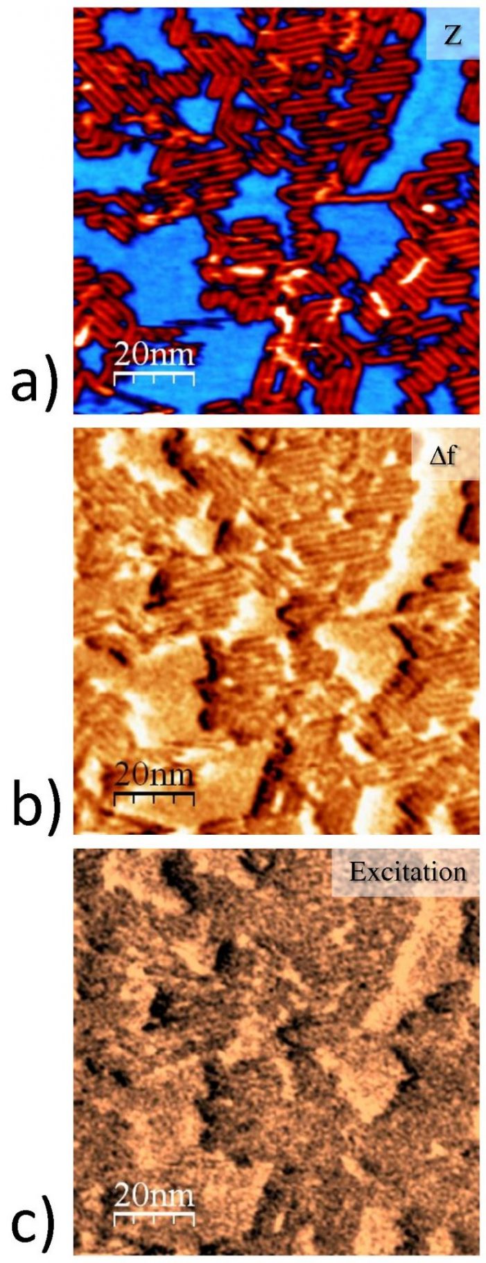
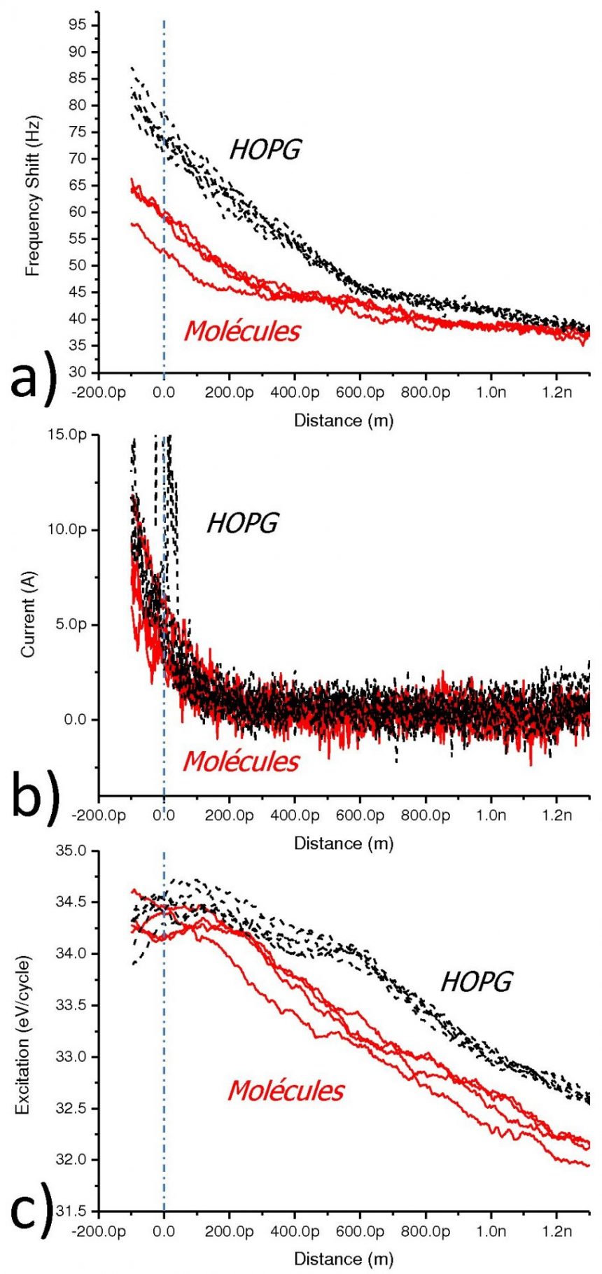
We studied the local properties of polymer chains composed of 3-dodecylthiophene (P3DDT) adsorbed on graphite [2]. In tunneling current distance regulation, we obtained the STM topography (Figure 2a)) but also the tip/surface force gradient (Figure 2b))) and dissipation (Figure 2c)) maps. Comparing these images, we highlight the inversed contrast between topography and force gradient. In other words, the tip of a STM feels repulsive forces when it scans above the adsorbed polythiophene molecules and on the graphite surface (Figure 3). Using the images obtained by tunneling current distance regulation and by frequency shift distance regulation, we quantified the dissipative interactions of several millielectronVolts/cycle at the scale of few P3DDT molecules. In parallel, the information provided by the frequency shift of the oscillating probe allows to quantify also the force gradients between the tip end and the surface. Hence, we observed by combined STM/FM-AFM, in a non-invasive way at room temperature, two dimensional clusters of P3DDT chains weakly adsorbed on graphite, with sub-tenth of nanometer oscillation amplitude [2]. These results are the first reported using such a probe on molecules at room temperature, and highlight the promising potential of this new microscope.
Figure 2: Images a) of topography, b) of frequency shift and c) of energy dissipation obtained in tunneling current distance regulation (<It>=4.3pA, Vtunnel=-1Volt ) for an oscillation amplitude of 92 picometers at a frequency of 35.9 kHz. In a), the P3DDT molecules appear as protruding lines (in red), parallel to the three dense directions of the atomic network of graphite (in blue). White lines correspond to second layer molecules. In b), the dark areas corresponding to low frequency shift are associated to the P3DDT molecules. In c), the energy dissipation mapping reveals that the dissipation is lower on the molecules areas.

Moreover, we used combined STM/FM-AFM imaging to characterize other systems such as the electroless growth of copper nanoclusters on insulating surfaces of polymers as Acrylonitrile-Butadiene-Styrene (ABS) and polyamide (PA) [3].
Presently, graphene foils on SiC samples are investigated with this new microscope in the frame of a PhD work which started recently in our team. The spin-offs of fundamental characterization of mechano-electronics coupling of molecular structures concern more particularly Molecular Electronics.
Figure 3: Approach spectroscopy curves a) in frequency shift, b) in tunneling current and c) in energy dissipation in different locations of the surface observed on figure 2. The red curves (continuous line) have been acquired on P3DDT molecular chains, the black curves (dashed line) have been recorded on clean graphite areas without molecules. The distance spectroscopy illustrates the repulsive behavior of the forces since the tunneling current apparition b), by the frequency curve a) acquired in the same time. Also, these results show that even for very low current setpoint (< 10 picoAmperes), the STM tip feels repulsive forces when it scans on weakly adsorbed P3DDT molecules or on the graphite surface. The curve c) allows to quantify a differential in energy dissipation of about hundred of meV/cycle, in the imaging conditions of figure 2 (vertical dashed blue line), between the clean graphite areas and the molecules areas.
References:
[1] Atomic force microscopy imaging using a tip-on-chip: Opening the door to integrated near field nanotools
J. Hayton, J. Polesel-Maris, R. Demadrille, M. Brun, F. Thoyer, C. Lubin, J. Cousty and B. Grévin, Review of Scientific Instruments 81, 093707 (2010).
[2] J. Polesel-Maris, Ch. Lubin, F. Thoyer, J. Cousty, “Combined dynamic STM and FM-AFM investigations on polythiophene chains on graphite with a tuning fork sensor”, sous presse dans Journal of Applied Physics (2011)
[3] Microscopic study of a Ligand Induced Electroless Plating process onto polymers
A. Garcia, Th. Berthelot, P. Viel, J. Polesel-Maris and S. Palacin, ACS Applied Materials & Interfaces 2(11), (2010) 3043.
Contact : Jerome Polesel.


