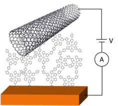
This work is based on photosensitive carbon nanotube transistors called OG-CNTFETs (optically gated carbon nanotube FETs) that we studied in details both as photo-detectors and as memory devices [2,3]. We showed that such devices can be used as a resistive memory elements [4] and proposed ways to implement them to store synaptic weights in neural network circuits [5,6]. The propose implementation is ideally suited for the parallel learning of multiple functions in a crossbar array of OG-CNTFETs as shown by simulations [5,6].
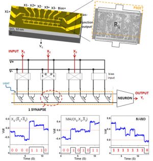
At the experimental level, using non-scaled down devices, we also showed that the same ensemble of 8 devices can be trained multiple times to code successively any 3-input linearly separable Boolean logic function despite device-to-device variability. This work represents one of the very few demonstrations of actual function learning with synapses based on nano-scale building blocks. [1] The potential of such approach for the parallel learning of multiple and more complex functions will be discussed. Finally we explore the scalability of such strategy by evaluating programming speed [7] and size issues [8] in single-nanotube based devices.
[1] K. Gacem et al., Nanotechnology 24, 384013, (2013)
[2] J. Borghetti et al., Adv. Mater. 18, 2535 (2006)
[3] C. Anghel et al., Nano Lett. 8, 3619 (2008)
[4] G. Agnus et al., Adv. Mater. 22, 702 (2010)
[5] W. Zhao et al., Nanotechnology 21, 175202 (2010)
[6] Liao et al, IEEE Trans. Circ. Syst. 58, 2172 (2011)
[7] G. Agnus et al., Small 6, 2659 (2010)
[8] D. Brunel et al., Adv. Funct. Mater. 23, 5631 (2013)

Such use of 3-terminal devices as resistive memory elements, while powerful from a function learning perspective, also has some limitations in terms of ultimate scaling. We thus also study 2-terminal memristors incorporating carbon nanotubes, not as switching medium, but as nano-scale electrodes [9].
This work is supported by the ANR (Panini ANR-07-ARFU-008 and Moorea ANR-12-BS03-004 Projects), the C’NANO IdF (Cinamon Project) and the EU (Nabab Project FP7-216777).
[9] Cabaret et al., submitted.