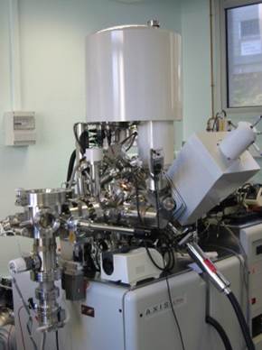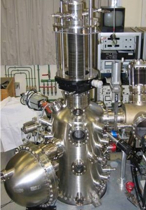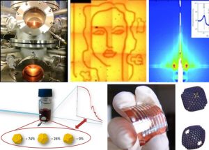

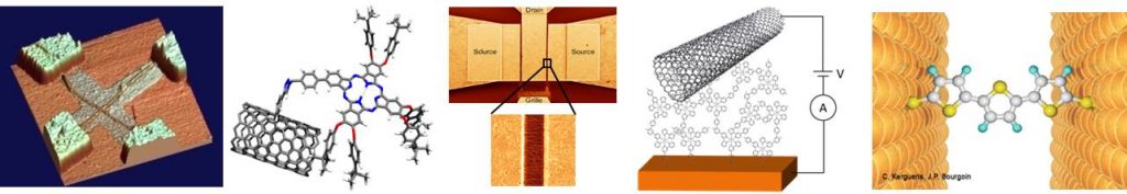
The LICSEN (Laboratory of Innovation in Surface Chemistry and Nanosciences) combines chemists and physicists (14 CEA staff members, 2 university associates, ~14 Ph.D students and postdoctoral fellows) around a core expertise in the field of chemical functionalization of surfaces and nanomaterials.
The main objective is to provide these surfaces and nanomaterials with additional properties of interest in the fields of sustainability, renewable energies and nanosciences for information and health technologies. Our studies expand from the understanding of chemical and physical mechanisms at the fundamental level up to the development of patented processes. The laboratory notably has strong interactions with industrial partners.


Learn more about our activities following the links below:
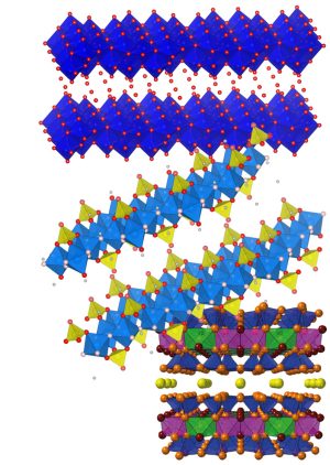
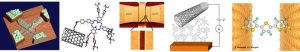
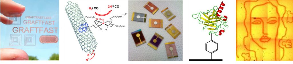
Surface Functionalization & Chemistry of Nanomaterials (Functionnalization processes (graftfast, SEEP…), nanomaterial grafting)
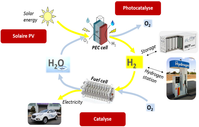
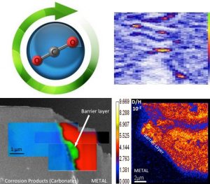
Materials for Energy (H2 fuel cells (PEMFC), Photovoltaic, Photo-electro-catalysis)
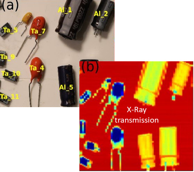
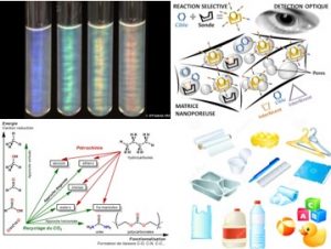
Sustainability & Recycling (Air and gas purification, Liquid-liquid and solid-liquid recovery processes, Joint CEA/NTU laboratory SCARCE)
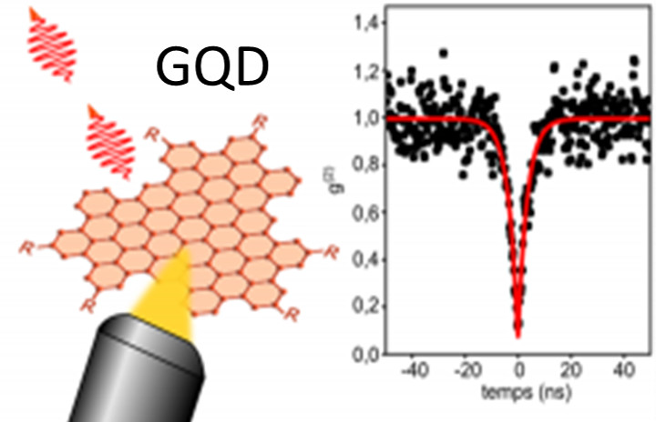
Nanomaterial Optics and Optoelectronics (Graphene Quantum Dots, Carbon nanotube optoelectronics, 2D Materials)
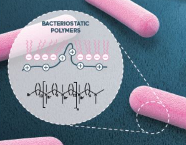
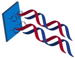
Surface Chemistry for Biology & Health (Functionnalized medical implants, Antibacterial surfaces)