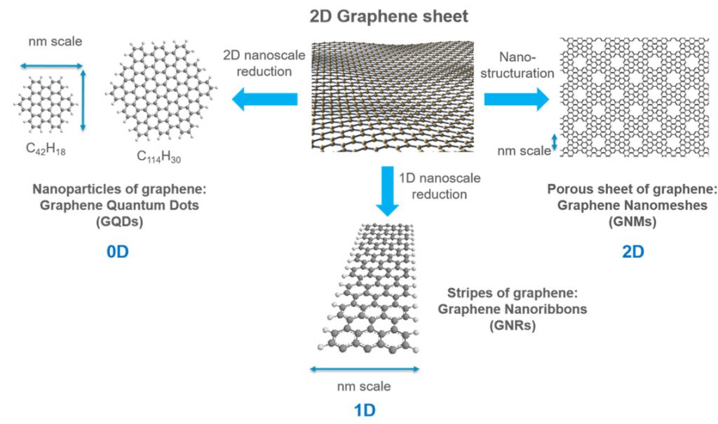
Nanostructuring graphene into 0D graphene quantum dots (GQD), 1D graphene nanoribbons or 2D nanomeshes allows opening a bandgap in its electronic structure
Main contact: Stéphane Campidelli
Graphene Quantum Dots Bottom-up Synthesis and optical properties
The outstanding electronic, optical and mechanical properties of graphene strongly inspire the scientific community. One of the main challenges for the use of graphene in devices is the control and modification of its electronic properties, and notably the controlled opening of a sizable bandgap. When a material is reduced to nanoscale dimensions, the confinement induces size-dependent properties. The reduction of one dimension of graphene down to the nanoscale leads to graphene nanoribbons (GNRs) while the reduction of the two dimensions leads to graphene quantum dots (GQDs), both having a bandgap. A great attention has been paid to the size reduction of graphene using conventional top-down approaches (lithography and etching, thermal treatments and oxidation of bulk materials). However, top-down approaches do not permit to manipulate the structure of the material at the atomic scale. In particular, they do not allow a sufficient control of the morphology and oxidation state of the edges, which drastically impact the properties. The resulting materials are inhomogeneous and their properties are largely impacted by defects. To truly control, with the required level of precision, the morphology and the composition of the materials and of its edges, the bottom-up approach is the relevant way to proceed.
Further reading: Fait-Marquant Iramis 2023 (in French) / Nature Communications 2023 / Nature Communications 2018 / BOGART Labex-project / GANESH ANR-project
Optical properties of chemically-sorted single-wall carbon nanotubes
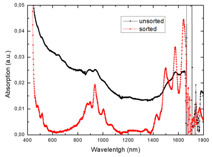
Single-walled carbon nanotubes have exceptional electronic and optical properties, but are unfortunately synthesized in the form of a poly-dispersed mixture of nanotubes of different length, diameter and chirality. Depending on their chirality, these SWNTs are either metallic or semiconducting. To use them in devices, it is necessary to extract from the mixture the nanotubes with the targeted properties. We are studying the optoelectronic properties of SWNTs at telecom (near-infrared) wavelengths, with a view to integrating them as light sources and detectors in photonic circuits integrated on the silicon platform. In particular, we have developed a highly selective method for the solution separation of semiconducting SWNTs with their fundamental optical transition centered at a wavelength of 1550 nm. These SWNTs are extracted via selective polymer adsorption and then connected into phototransistors directly on silicon waveguides. In particular, we have demonstrated that these devices combine electro-emission and photodetection functions.
Further reading : Scientific Reports 2018 / Adv. Funct. Mater. 2017 / CARBONIC ANR-project / CARTOON FP7-project
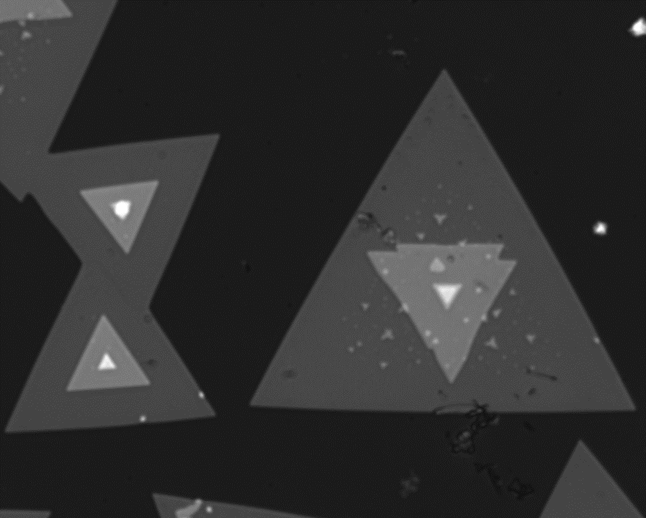
Monolayers, bi- and tri-layers of MoS2 grown by CVD at Licsen and observed by optical microscopy using an anti-reflective substrate (Ullberg et al. 2023)
Main contact: Vincent Derycke
2D materials synthesis and optoelectronic properties
Our work on 2D materials includes the synthesis of MoS2 and other TMDs by CVD, their intergartion in field-effect transistors (FETs) and photo-tranisitors (alone or combined with a post-functionnalization step using perovskite NPs), the study of microscopy techniques for high-contrast observation of both their morphology and charge density.
We also worked intensively on graphene oxide chemistry, deposition and observation methods.
Further reading : ACS Nano 2024/Nanoscale 2019 / Nathan Ullberg thesis / Nouvelle microscopie optique très haute sensibilité pour l’observation des nanomatériaux bidimensionnels (in French) / MoS2 Transistors with Ultrathin and Robust Organic Gate Dielectric
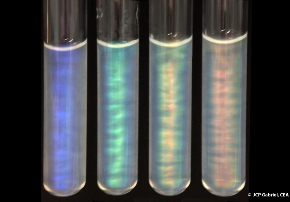
Visible light diffracted by different lamellar periods of colloidal suspension of H3Sb3P2O14 in water (shortest => Blue; longest => red)
© JCP Gabriel, CEA.
Main contact: Jean-Christophe Gabriel
Exfoliated 2D materials for purification and analysis
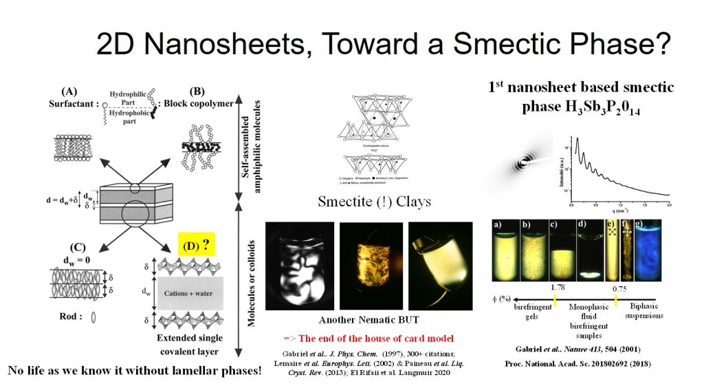
In our laboratory, we synthesize and characterize low dimensionality materials (0, 1 and 2D), by all means necessary and available. These materials can often be exfoliated/dispersed in solution leading to some complex/colloidal fluids, exhibiting a very wide range of fascinating behaviors. In 2001, we discovered the first lamellar phase based on extended 2D nanosheets, and further confirmed it recently.
Thanks to the awarded ANR Project 4WATER (2018), we are elaborating new and cheap multi-target chemical sensor arrays for the continuous monitoring of groundwater quality. Using a microelectronic approach, the sensors will be based on functionalized nanomaterials and that will target various ions selected for their relevance as regards the quality of fresh water.
Thanks to the awarded ANR Project 2D-MEMBA (2021): we integrate nanomaterials for the making of less power-hungry membranes for the purification of water
