14/11/2017 - Inauguration du Laboratoire Commun CEA-PROTEC Industrie (projet ANR Labcom' Mestrel)
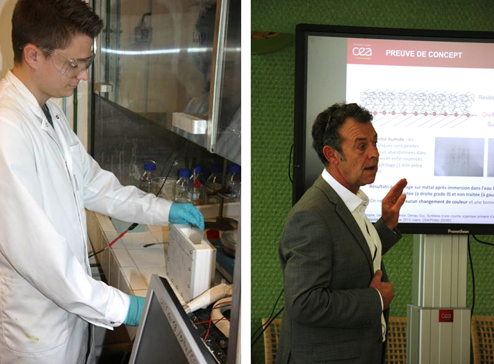 Mercredi 14 novembre, Le CEA-Licsen et la société PROTEC Industrie inauguraient leur laboratoire commun MESTREL pour mettre au point un procédé de préparation de surface avant peinture sans produits chimiques cancérogènes, mutagènes ou reprotoxiques, destiné en particulier à l’aéronautique. Ce projet est soutenu par l'ANR au travers du projet "LabCom Mestrel".
05/10/2017 - Thèse d'Andrea Falconi
 ► La soutenance de thèse d'Andrea FALCONI « Modélisation électrochimique du comportement d’une cellule Li-ion pour application au véhicule électrique » aura lieu le Jeudi 5 octobre 2017 à 10h30 à l'INSTN (CEA Saclay). (Contact: R. Cornut).
26/09/2017 - Seminar by Dr. Sylvain Clair (Aix-Marseille Université, CNRS, IM2NP)
 ► Sylvain Clair from TAix-Marseille Université, CNRS, IM2NP will give a seminar entitled « Surface-supported covalent organic networks » at 11 am on September 26, Room 26 building 127. (Contact: S. Campidelli).
15/09/2017 - Thèse de Quentin Arnoux - UPMC Jussieu 10h
 ► La soutenance de thèse de Quention Arnoux « Caractéristiques électroniques et structurelles d'une interface oxyde conductrice / organique transparente : vers les applications pour des dispositifs électroniques organiques » a eu lieu le vendredi 15 septembre 2017 à 10h à l'UPMC (Jussieu), Salle 101 T32-42 1er étage. (Contact: L. Tortech).
14/09/2017 - Seminar by Prof. Andreas Klein from TU Darmstadt (Germany)
 ► Apl. Prof. Dr. Andréas Klein from TU Darmstadt (Germany) gave a seminar entitled « Electronic Structure Analysis of Functional Oxides using XPS » at 3pm on September 14, Room 26 building 127. (Contact: L. Tortech).
28/08/2017 - Crystalline metamaterials for topological properties at subwavelength scales
► 3D printing and polymer metallization at LICSEN (contact: Thomas Berthelot) was use to help Institut Langevin to develop new metamaterials. The work by Simon Yves (Institut Langevin), Romain Fleury (Institut Langevin & EPFL), Thomas Berthelot (CEA/Nimbe/Licsen), Mathias Fink (Institut Langevin), Fabrice Lemoult (Institut Langevin) & Geoffroy Lerosey (Institut Langevin) was published in July in Nature Communications 8, 16023 (2017).
17/07/2017 - HDR de Géraldine Carrot
► Lundi 17/07 à 14h à Neurospin, Géraldine Carrot a présenté ses travaux d'HDR intitulés: « Nanostructures hybrides et polymères : construction, contrôle et perspectives en biologie ».
07/07/2017 - Visit of Pr. Takuya Matsumoto from Osaka University, Japan
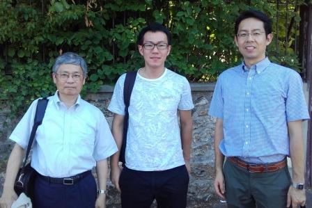
On July 7, LICSEN hosted the visit of Pr. Takuya Matsumoto, Dr. Yoichi Otsuka and Kento Araki from the Osaka University, Department of Chemistry, Graduate School of Science. The notably presented two seminars:
► Talk 1 : I-V characteristics of Ru-complex monolayers probed by conductive AFM
► Talk 2: Time-resolved electrostatic force microscopy
Learn more about Pr. T. Matsumoto's Laboratory (Chemical Kynetics and Dynamics) here.
06/07/2017 - Nanotube-based light sources and detectors at telecom wavelength
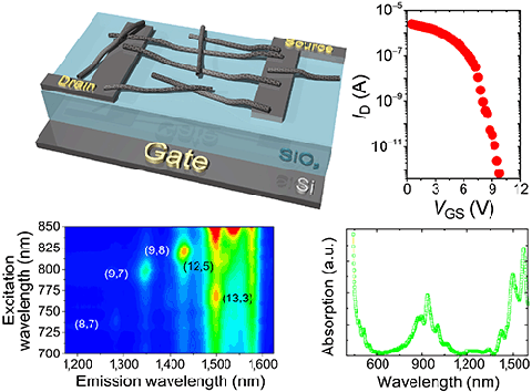
Within the recently completed European FET-Open CARTOON project, the consortium studied carbon nanotube based devices for infrared light emission and detection at telecom wavelength and their coupling to silicon waveguides. Contact: arianna.filoramo@cea.fr
Related publications:
Polarization-sensitive single-wall carbon nanotubes all-in-one photo-detecting and emitting device working at 1.55µm, Adv. Funct. Mater. (2017).
Integration of Carbon Nanotubes in Silicon Strip and Slot Waveguide Micro-Ring Resonators, IEEE Trans. on Nanotech. 15, 583 (2016).
High selective sorting of semiconducting single walled carbon nanotubes for light emission at telecom wavelengths, Nano Research 9, 2478 (2016).
Diameter-Selective Dispersion of Carbon Nanotubes via Polymers: A Competition between Adsorption and Bundling, ACS Nano 9, 9012 (2015).
30/06/2017 - Conductivity of monolayer MoS2 measured by Electrochemicl Microscopy
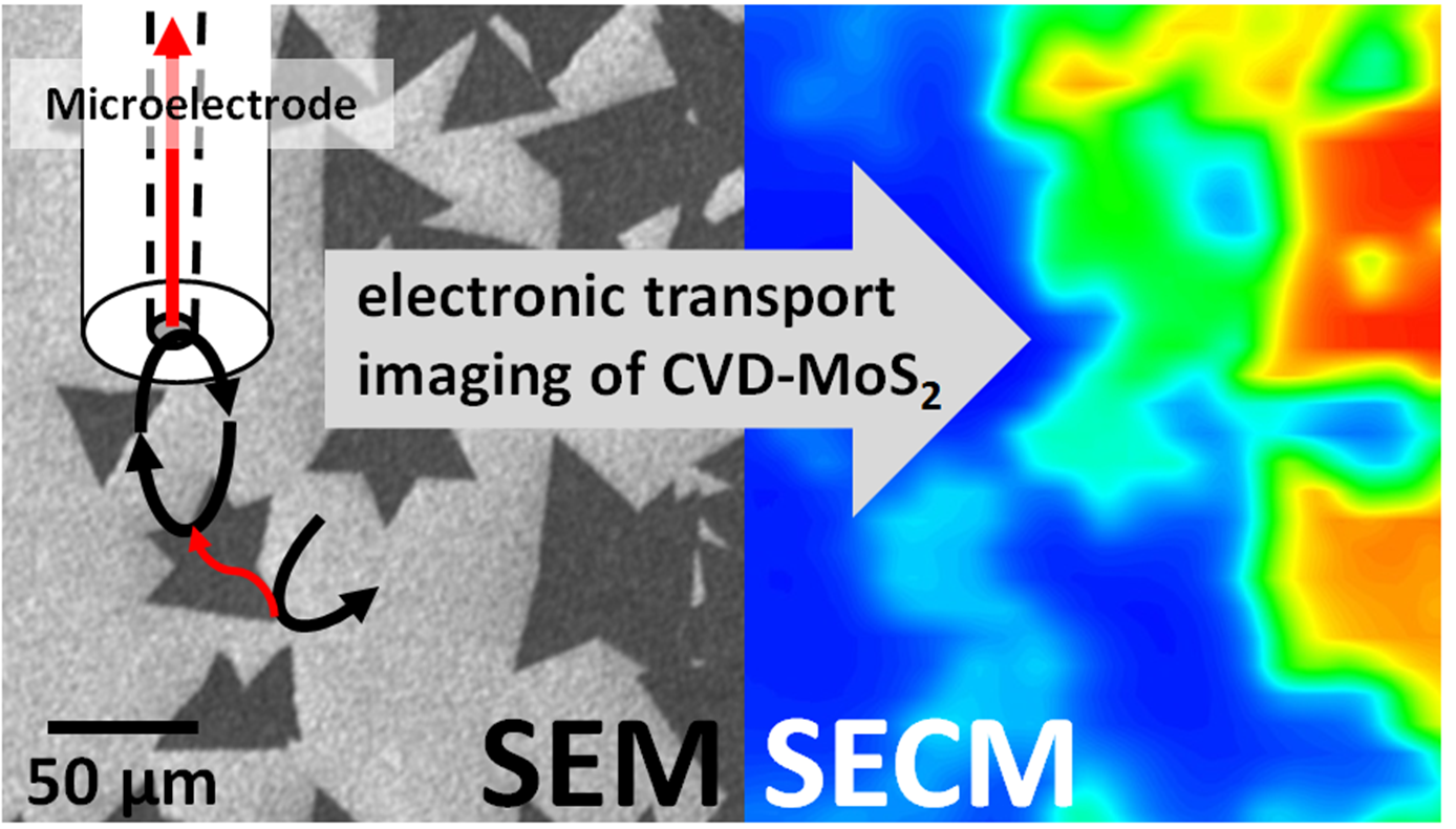
Electronic transport of MoS2 mono-layered flakes investigated by scanning electrochemical microscopy by O. Henrotte, T. Bottein, H. Casademont, K. Jaouen, T. Bourgeteau, S. Campidelli, V. Derycke, B. Jousselme and R. Cornut, ChemPhysChem 2017.
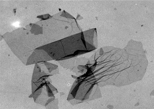
The amazing properties of 2D materials are envisioned to revolutionize several domains such as flexible electronics, electrocatalysis, or biosensing. Herein we introduce Scanning Electrochemical Microscopy (SECM) as a tool to investigate molybdenum sulfide in a straightforward fashion, providing localized information regarding the electronic transport within CVD-grown micrometric size crystalline single-layers of MoS2. Our investigations show that within flakes assemblies some flakes are well electrically interconnected, with no detectable contact resistance, while others are not electrically connected at all independently from the size of the physical contact between them. Overall, the work shows how the complex electronic behavior of MoS2 flake assemblies (semiconducting nature, contact quality between flakes) can be investigated with SECM. Contact: renaud.cornut@cea.fr
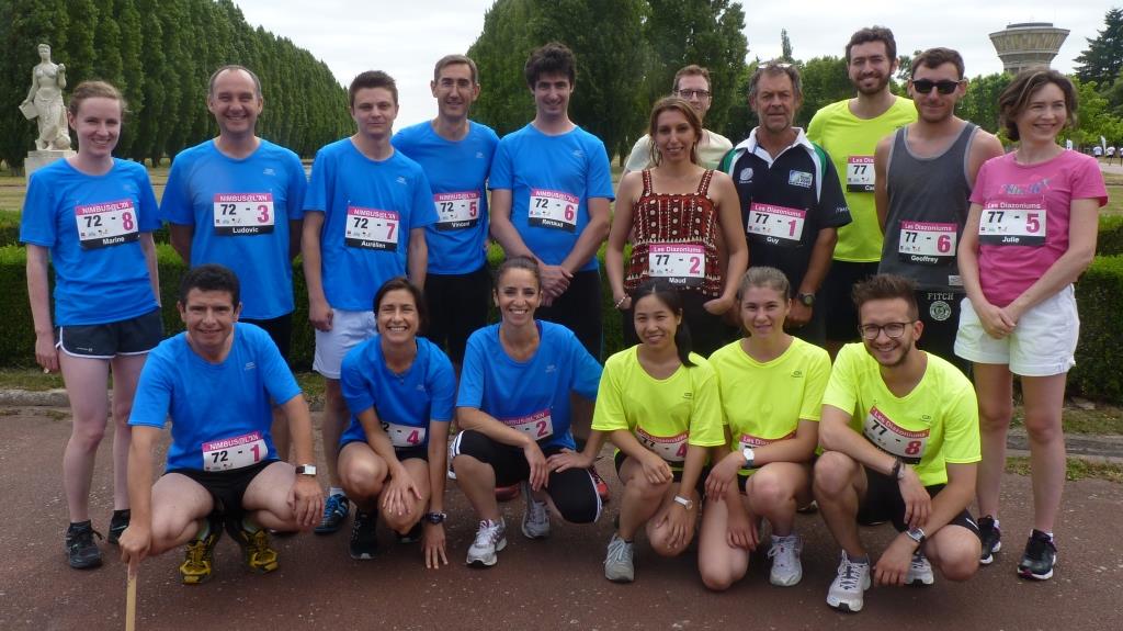
23/06/2017 - Course CEA
Un grand bravo aux deux équipes de relayeurs du LICSEN et merci à leurs nombreux supporters !
12/05/2017 - A new optical microscopy technique to "see" 2D nanomaterials
 ► Researchers at CEA-Licsen, CNRS-Le Mans, CNRS-Marseille and Université Libanaise developped a new optical microscopy technique called BALM (Backside Absorbing Layer Microscopy) able to image 2D materials (such as graphene oxide) with high resolution and to follow chemical reactions at surfaces in real time. The study is published this month in Science Advances. It was also commented in NanotechWeb.
voir les ARCHIVES 2016
voir les ARCHIVES 2014-2015
