


2007
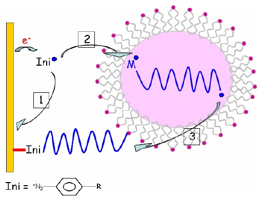
Electrografting of vinylic polymers onto conducting surfaces has historically been achieved via a direct electron transfer from the cathode to the electro-active monomers in solution. The resulting radical-anion, together with the anions that allow the propagation of the growing grafted polymer chains, are highly sensitive to proton sources. The "classical" cathodic electrografting process thus requires strictly anhydrous conditions.
Radical polymerization does not suffer the same drawback and is easily performed in aqueous conditions. We thus demonstrated that cathodic electrografting on conducting surfaces can be achieved in protic conditions, provided the polymerization is radically initiated by an electro-active moiety. The best initiators are actually diazonium salts.
Indeed, as shown by Pinson, diazonium salts can be easily electro-grafted on conducting substrates by cathodic reduction to phenyl radical species in mild conditions. However, when the applied potential is higher than the reduction potential of the diazonium salt, a significant part of the resulting phenyl radicals are diverted to the solution and may act as initiators of radical processes. We demonstrated that this initiation is efficient and delivers polymer chains from vinylic monomers solubilized within the electrolyte (either directly or in micellar conditions). The resulting polymer chains normally grow in solution or within the micelles, and are eventually terminated by any radical or radical scavenger present in the medium. Among the termination processes, the most interesting is the reaction of the growing polymer chains with the already grafted aromatic rings coming from the direct electrografting of the diazonium initiator. Hence, the diazonium salt acts both as an initiator for the radical polymerization in solution, and as a primer for the chemical grafting of the resulting polymer chains on the surface of the electrode.
Angle-resolved XPS analysis confirmed that the polyphenylene grafted films arising from the direct electrografting of the diazonium moieties are actually located below the vinylic chains, in direct contact with the electrode.
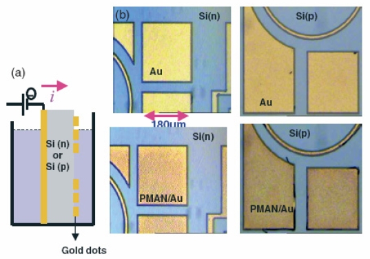
The localized grafting, at a micronic or submicronic scale, of organic substances on surfaces is often a prerequisite in the design of bioelectronics devices, and a valuable component of some combinatorial screening strategies. Moreover, microelectronic devices including transistors, sensors or memories are generally based on interfaces between conducting and quasi-insulating domains resulting from lithographic steps, ionic implantation and silicon oxide thermal growth. Most of these techniques require many steps of transformation and their implementation is often expensive.
We developed a one step technique that allows the localized electrografting of organic matter on designed areas of a composite conducting surface. This method relies on the local work function of electrons, which can easily be tuned by patterning different conducting materials on the substrate. [1-2]
The method was originally demonstrated through examples of composite gold/silicon substrates, which underwent organic electrografting only on gold parts, even when the potential was applied via the silicon substrate and the gold parts were geometrically isolated from the voltage source. That effect is due to:
• The mechanism of cathodic electrografting, which is initiated by an adsorbed radical-anion resulting from a direct electron-transfer from the cathode to electro-active molecules
• The weaker work function of gold with respect to silicon (in solution), which leads to more efficient "output" kinetics from the golden areas.
The generation of highly spin-polarized electron currents is one of the dominant focusses in the field of spintronics. For this purpose, spin filtering is one very interesting phenomenon, both from a fundamental and from a technological standpoint, that involves the spin-selective transport of electrons across a magnetic tunnel barrier. Successful spin filtering at room temperature could potentially impact future generations of spin-based device technologies not only because spin filters may function with 100% efficiency, but they can be combined with any non-magnetic metallic electrode, thus providing a versatile alternative to half-metals or MgO-based classic tunnel junctions. The spin filter effect originates from the exchange splitting of the energy levels in the conduction band of a magnetic insulator. As a consequence, the tunnel barrier heights for spin-up and spin-down electrons are not the same, leading to a higher probability of tunneling for one of the two spin orientations.
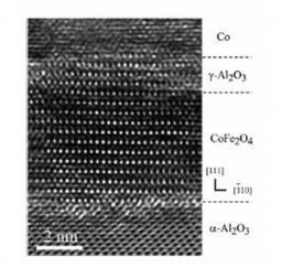
CoFe2O4 is a very promising candidate for room temperature spin filter applications thanks to its high Curie temperature (TC=793 K) and good insulating properties. Electronic band structure calculations from first principles methods predict CoFe2O4 to have a band gap of 0.8 eV, and an exchange splitting of 1.28 eV between the minority (low energy) and majority (high energy) levels in the conduction band , thus confirming its potential to be a very efficient spin filter, even at room temperature. In order to accurately demonstrate the spin filtering capabilities of CoFe2O4 up to room temperature, we have prepared CoFe2O4(111)/γ-Al2O3(111)/Co(0001) fully epitaxial tunnel junctions by oxygen plasma-assisted molecular beam epitaxy (MBE) on Pt(111) underlayers. In this system, the spinel γ-Al2O3 serves to decouple the CoFe2O4 and Co magnetic layers. Before any spin-polarized transport measurements were performed on the full MTJ system, our CoFe2O4(111)/γ-Al2O3(111) tunnel barriers were carefully characterized by a wide range of techniques in order to optimize their structural and chemical properties. Fig.1 shows a high resolution transmission electron microscopy (HRTEM) study demonstrating the high crystalline quality of our CoFe2O4 (5 nm)/γ-Al2O3 (1.5 nm)/Co (10 nm) multilayers. In particular, we observe near perfect epitaxy in the single crystalline CoFe2O4(111)/γ-Al2O3(111) tunnel barrier, which is a consequence of the optimized growth conditions and the spinel structure of both constituents.
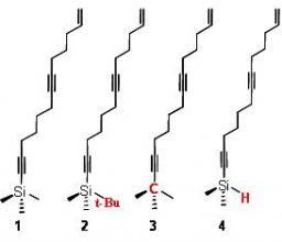
We discovered in 2002 (JACS 124, 9998, 2002) that the linear multifunctional trimethylsilyl-acetylene 1 ,TMSA, (schema 1) forms long-range and highly stable self-assembled monolayers (SAMs) on reconstructed Au(111). In order to better understand the interactions governing self-assembly in this new system, we synthetized a series of homolog organosilanes and performed STM observations at the Au(111)/n-tetradecane interface.
Collaborations with LNIO, P. Royer dir., Université de technologie de Troyes
Laboratoire EM2C, J.-J. Greffet dir., École Centrale de Paris
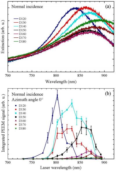
The reduction below the wavelength of light of the size of a metallic object induces important modifications of its response to an optical excitation. One of the most dramatic effects is the emergence of collective electron oscillations modes, known as localized plasmons. For noble metals, these resonances are in the visible or near-infrared range of the spectrum. Plasmon resonances allow for the confinement of optical fields over lengths below the diffraction limit and thus yield strong local enhancements in terms of local electromagnetic fields (classical view) or density of electromagnetic modes (quantum view). The resulting Purcell effects play essential roles in the interaction of molecules with electromagnetic fields, of particular importance in our studies of STM-tip induced luminescence or tip-induced non-linear optical processes (see the corresponding sections).
We have investigated plasmonic effects occurring in specifically designed metallic nano-object and realized by electron beam lithography (EBL). The determination of the spatial distribution of the optical near field at object resonances is commonly addressed by scanning near field optical microscopy (SNOM). While offering a field mapping at lateral resolution down to tens of nanometers, the measurement proceeds by the insertion of a probe in the immediate vicinity of the object, making its intrinsic optical characterization complex due to possibly strong tip / object coupling. As an alternative probing tool, we use photoemission electron microscopy (PEEM) in the multiphoton regime. By collecting the electrons emitted by metal nanoobjects under illumination, two-dimensional intensity maps reflecting the distribution of the optical near-field can be obtained. The imaging technique exploits well established electron optics, i.e. involves no physical probe altering the measure. In that way, optical phenomena are observed with a lateral resolution close to 50 nm.
Collaboration with Collège de France, M.-P. Teulade-Fichou
Fluorescent labeling of DNA :
Technical support : F. Merlet
Collaboration with Laboratoire de Chimie des Polymères, A.-J. Attias
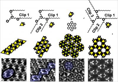
The spontaneous ordering and assembly of molecules on well-defined surfaces constitutes a promising bottom-up route in our quest for atomically-precise fabrication of functional molecular architectures. We have developed an original approach to the design of self-assembling building blocks tailored so as to form on demand specific hierarchical topographies.
Based on our long-term experience on self-assembly of triphenylene-cored columnar liquid crystals [1], we conducted a systematic analysis of the important role played by substrate interactions [2]. This led us to a generalization of the 2D molecular sieves [3]. We designed a new molecular unit acting as a functional linking group able to form strong surface-assisted intermolecular “clips”. These non-covalent bondings are based on an interdigitation of alkyl side-chains which strictly mimics alkane epitaxial assembly on HOPG. We have thus realized various target topologies: mono- bi- and tri-functional molecules building blocks forming dimers, chains or 2D networks respectively, each entity further assembling in the most compact structure.
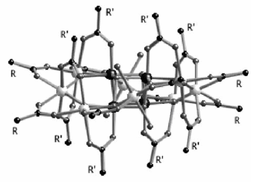
Polynuclear complexes that possess a large spin ground state associated with strong magnetic anisotropy have attracted much attention during the last decade. Such complexes have a magnetic bistability that can be associated to a single molecule. They are called Single Molecule Magnets (SMM).
Among SMMs, the so called Mn12 is still the most studied since it possesses the highest blocking temperature below which bistability occurs. These molecules may be integrated in a device for information storage; quantum calculation may be envisaged as well because Quantum Tunneling of the Magnetization (QTM) was evidenced in some systems.
The very early stage before building molecular devices is to manage manipulating small amounts of molecules and to study their magnetic properties individually. One of the first steps is to achieve systems where a small collection of molecules can be studied. We have chosen to graft them on silicon surfaces.
Mn12 has already been deposited on various surfaces using (i) the Langmuir–Blodgett technique, (ii) spontaneous grafting on gold by using a thiol-modified Mn12 complex, (iii) deposition of the biphenyl derivative of Mn12 and nanopatterning on polycarbonate films …None of those techniques allows controlling the orientation of the Mn12 moiety. We demonstrated that by using a mixed Mn12 complex (i.e. containing two different carboxylate groups) it is possible to graft a monolayer in an oriented manner on a silicon substrate.
We selected a Mn12 complex possessing dichloroacetate groups in axial positions and tert-butyl acetate groups in equatorial positions. That complex was allowed to interact with silicon substrates bearing chemically grafted carboxylic units (obtained from thermal grafting of undecylenic acid on Si-H(100) surfaces). ATR-FTIR spectra show that the carboxylic band at 1718 cm-1 almost vanishes after the immersion of the substrate in the Mn12 solution, which is the first evidence for the grafting of molecules by carboxylate substitution.
The exact contribution from the contact conductance has been much less investigated, mainly because the thiol-gold couple overwhelms the other interface linkages in literature, and also because comparison experiments are quite difficult.
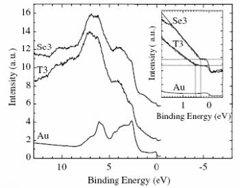
First, density functional theory calculations were used to show that the two molecules isolated in vacuum have quite a similar electronic structure. In particular, their calculated ionization potentials differ by less than 1%, revealing the absence of a significant difference between the two molecules when isolated in vacuum. The electronic density representation of the orbitals confirms this similarity. This suggests to interpret our STM results as a direct consequence of a difference in adsorption of Se3 and T3 onto gold due to their different coupling groups.
Then, ultraviolet photoelectron spectroscopy (UPS) was used to study SAMs of pure T3 or Se3 were prepared onto gold substrates. T3 and Se3 spectra show a good similarity with that of thick terthiophene, which means that the electronic structure of the adsorbed molecules core remains largely undisturbed by the adsorption onto the metallic surface.
However, tiny but significant differences nevertheless exist between T3 and Se3 SAMs spectra. In particular, the two peaks at lower energy are shifted towards higher energies by about 0.2 eV in the case of T3 compared to Se3. (Fig. 1)
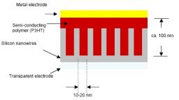
Most solar cells industrially produced are currently based on silicon wafers (93.5 %). As a result, the price of photovoltaic modules is very high (5.6 €/Wp at its lowest in 2004) and is still expected to increase, due to a fast growing demand and a shortage in silicon production. Moreover, single-crystal silicon solar cells, which have a power conversion efficiency of more than 20 %, are heavy and fragile, which prevents them from being used for mobile applications.
Several concepts have been developed to tackle these problems. Inorganic thin film devices (based for example on amorphous silicon or CuInGaSe2) have reached efficiencies above 12 % and enter commercial stage. Organic solar cells are on the other hand expected to show lower production costs and easier integration on flexible substrates. Yet they still have low efficiencies (around 5 % at best) and suffer from short lifetimes as compared to inorganic devices.
Nanostructured materials are considered one of the best ways to improve the efficiency of organic and hybrid solar cells. Indeed, devices based on such materials have an increased interface area and a reduced average distance from one point to an interface. As the separation of charge carriers occurs at interfaces, such structures enhance it, and thus lead to an increase in the photocurrent. Bulk heterojunctions between polymers and inorganic nanoparticles lead to efficiencies of 1.8 % (with MDMO-PPV and branched CdSe nanoparticles). Devices, where nanostructured materials are directly grown on the substrate, would additionally bring an electrically continuous path from the active interface to the electrodes.[1]
The project aims at demonstrating the relevance of this approach by making devices (Fig. 2) based on silicon nanowires directly grown on a transparent conductive oxide, and poly(3-hexylthiophene), which shows one of the highest hole mobility among semi-conducting polymers (0.1 cm2.V-1.s-1).
The localized grafting, at a micronic or submicronic scale, of organic substances on surfaces is often a prerequisite in the design of bioelectronics devices, and a valuable component of some combinatorial screening strategies. Moreover, microelectronic devices including transistors, sensors or memories are generally based on interfaces between conducting and quasi-insulating domains resulting from lithographic steps, ionic implantation and silicon oxide thermal growth. Most of these techniques require many steps of transformation and their implementation is often expensive.
We developed a one step technique that allows the localized electrografting of organic matter on designed areas of a composite conducting surface. This method relies on the local work function of electrons, which can easily be tuned by patterning different conducting materials on the substrate. [1-2]
The method was originally demonstrated through examples of composite gold/silicon substrates, which underwent organic electrografting only on gold parts, even when the potential was applied via the silicon substrate and the gold parts were geometrically isolated from the voltage source. That effect is due to:
• The mechanism of cathodic electrografting, which is initiated by an adsorbed radical-anion resulting from a direct electron-transfer from the cathode to electro-active molecules
• The weaker work function of gold with respect to silicon (in solution), which leads to more efficient "output" kinetics from the golden areas.
We study electro-grafted films on metal substrates as a solution for the dry lubrication of low-level electric contacts. At the moment low-level electric contacts are lubricated by means of liquids lubricants but this solution is not satisfactory for many reasons and electrical contacts still remain the weakest point of electrical circuits and a main source of failure. Among the degradation phenomena that occur in traditional liquid lubricated electrical contacts are oxidation, wear, overheating and fretting (oxidation and premature wear caused by mechanical vibrations). Many of those phenomena are caused by liquid lubricants displacement or its degradation, leading to unprotected metal-to-metal contacts.
Moreover with the increasing miniaturization of device components and high-performance materials, the surface-to-volume ratio increases, and the properties of the surfaces become increasingly more important. In many cases, especially in aerospace, high-temperature, and computer applications, it is also impractical or undesirable to have a liquid lubricant present, and one has to rely entirely on the tribological properties of dry surfaces.Therefore the functionalization of metallic surfaces with organic molecules to impart “lubricating” properties becomes a subject of major interest both from fundamental and technological points of view.
With respect to other techniques for grafting organic molecules on metal surfaces (SAM, Langmuir-Blodgett films, …) electrografting allows the formation of strong covalent bonds at the organic/inorganic interface leading to the formation of highly-adherent thin-films (thickness < 50nm). The electrografting of fluorinated molecules (fluorinated diazonium salts or fluorinated methacrylates) allows obtaining robust films providing low-friction properties.
As those films are naturally insulating, the necessary electrical transport through the metal-organic-metal interface can be borne by adding a conducting or semi conducting charge to the films. In particular we concentrate on carbon nanotubes networks and on conducting fluorinated PEDOT.
Our early results on grafted fluorinated polymethacrylates films show excellent behaviour in term of stability and tribological properties, reaching friction coefficient as low as 0.1 and showing wear resistance in severe testing conditions. (Fig. 1).
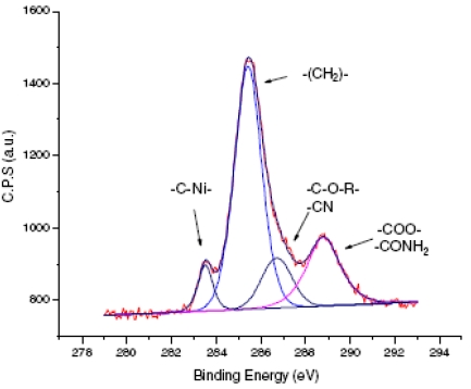
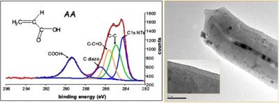
Cathodic electropolymerization has already proven its ability to produce robust and conformal organic films chemically grafted on metallic and semiconducting surfaces used in various domains such as microelectronics, biomedical applications, soldering, chemical waste treatment or corrosion protection. Contrary to the electrodeposition of semi-conducting polymers like polypyrrole or polyaniline, strong covalent bonds between the cathode and the polymer film area created during the process, as indirectly proved by numerous studies including chemical post-treatments, electrografting on rotating electrodes or mechanical measurements. A direct evidence can however be obtained from XPS.
Probing the chemical interface between a polymer film and a metallic substrate is very difficult. Indeed, the interface is "buried" under the polymer film and thus difficult to reach. For instance, XPS cannot probe more deeply than ca. 15 nm below the outmost surface. It is thus necessary to limit the growth of the polymeric film to be able to probe the interfacial signature.
This was done by using a redox active molecule that cannot polymerize. Indeed, with classical vinylic monomers such as acrylonitrile or methyl methacrylate, the grafting step that immediately follows the electron transfer from the cathode, gives a very unstable species bearing a negative charge very close to a negatively charged electrode. The instability is classically relaxed by the polymerization that moves away the charged species from the electrode.
With crotononitrile, another relaxation route is possible through a proton transfer that "heals" the carbanion before polymerization occurs. Hence, ultrathin grafted films are obtained. XPS analysis of the resulting films allows the direct observation of the carbon-metal bond that is buried under the grafted film and contributes greatly to its robustness. A clear and distinct peak at 283.5 eV is observed which is attributed to C-Ni bonding. Its full width at mid-height is only 0.8 eV, which indicates that the bonding is probably perpendicular to the surface.
Contact: G. Deniau
Refrences:
[1] Carbon-to-metal bonds: Electrochemical reduction of 2-butenenitrile
Guy Deniau, Laurent Azoulay, Pascale Jégou, Gilles Le Chevallier and Serge Palacin, Surface Science, 600 (2006), 675.
[2] G. Deniau et al., Patent FR2883299, 15/03/2005
Electrografting of vinylic polymers onto conducting surfaces has historically been achieved via a direct electron transfer from the cathode to the electro-active monomers in solution. The resulting radical-anion, together with the anions that allow the propagation of the growing grafted polymer chains, are highly sensitive to proton sources. The "classical" cathodic electrografting process thus requires strictly anhydrous conditions.
Radical polymerization does not suffer the same drawback and is easily performed in aqueous conditions. We thus demonstrated that cathodic electrografting on conducting surfaces can be achieved in protic conditions, provided the polymerization is radically initiated by an electro-active moiety. The best initiators are actually diazonium salts.
Indeed, as shown by Pinson, diazonium salts can be easily electro-grafted on conducting substrates by cathodic reduction to phenyl radical species in mild conditions. However, when the applied potential is higher than the reduction potential of the diazonium salt, a significant part of the resulting phenyl radicals are diverted to the solution and may act as initiators of radical processes. We demonstrated that this initiation is efficient and delivers polymer chains from vinylic monomers solubilized within the electrolyte (either directly or in micellar conditions). The resulting polymer chains normally grow in solution or within the micelles, and are eventually terminated by any radical or radical scavenger present in the medium. Among the termination processes, the most interesting is the reaction of the growing polymer chains with the already grafted aromatic rings coming from the direct electrografting of the diazonium initiator. Hence, the diazonium salt acts both as an initiator for the radical polymerization in solution, and as a primer for the chemical grafting of the resulting polymer chains on the surface of the electrode.
Angle-resolved XPS analysis confirmed that the polyphenylene grafted films arising from the direct electrografting of the diazonium moieties are actually located below the vinylic chains, in direct contact with the electrode.
Due to their outstanding properties (Young modulus E = 45 GPa, conductivity = 1 GA cm-2), carbon nanotubes (CNTs) have recently subjected lot of attraction. Indeed, CNTs find applications in different topics such mechanical reinforced composite materials, microelectronics, and biology for example. However, CNTs are poorly soluble and prone to aggregation in bundles.
Thus, processing of CNTs is a key point for future applications and requires appropriate chemical modification. Among the numerous methods published in recent literature for functionalizing CNTs, chemical and electrochemical grafting appear the most frequent. In particular, atom transfer radical polymerization (ATRP), covalent anchoring of preformed polymer chains and electrografting of diazonium salts on CNTs have recently been reported.
We first studied cathodic electrografting on CNTs using the Surface Electroinitiated Emulsion Polymerization (SEEP) process, where diazonium salts are used both to initiate the radical polymerization of vinylic monomers in solution and to form a primer grafted polyphenylene like layer on the carbon surface. SEM and TEM analysis revealed that ultrathin polymer films are grafted on carbon nanotubes sidewalls. XPS spectroscopy further confirmed the functionalization of multi-walled carbon nanotubes.
Electrografting is a powerful technique that allows true chemical modification of conducting and semi-conducting surfaces. [1] Indeed, injecting electrons from the bulk material towards a solution of suitable electroactive molecules leads to the formation of activated moieties in the vicinity of the electrode, which eventually form strong chemical links with the electrode.
Our group has historically been developing the electrografting of vinylic polymers via an electro-induced anionic polymerization that starts from a precursor chemically bound to the electrode.
Strong efforts were devoted in past years both to the theoretical interpretation of the mechanism and towards practical applications of the process. That latter approach was rewarded in 2001 by the creation of a spin-off company, Alchimer, which applies the process in the biomedicine and microelectronics fields. [2-13]
From that moment, our group carried on support activities to develop and enrich the electrografting process. We first demonstrated that biological moieties can be directly immobilized on electrografted polymethacrylonitrile films via a spontaneous reaction between the nitrile groups from the film and the amino groups from the amino acids of the protein, in alcoholic basic medium. The formation of the resulting imino-ethers groups was followed by XPS measurements and assessed by high precision calculations of core electron binding energies. The final protein film is stable toward aqueous rinsing and can be used for protein-substrate recognition. [14]
As CMOS goes towards 65nm technology node, the integration of traditional memory cells such as DRAMs and non-volatile Flash gets limited. The solutions proposed for their replacement (FeRAM, MRAM, PCM) show a large energy consumption. Therefore there is still a need for a high-density and ultra low-power memory devices suited to respond to the growing market of wireless Systems On a Chip (SOC). For this purpose, the concept of Negative Differential Resistance memory (NDR) based on Resonant Tunneling molecular Diode (RTD) appears very promising. Indeed, with one of the electrodes a semi-conductor, one can take benefit of the localized density of states.
The "heart" of the device is indeed the interface linkage between the electrode and the molecule, together with the order within the monolayer. Molecules with a σ−π−σ sequence have already been derived from molecular orbital calculations in order to allow significant electron transfer from silicon at moderate voltage (below 3V). Those tri-block molecules were chemically grafted onto hydrogenated silicon surfaces (Si-H) and the resulting monolayers were fully characterized by IRRAS, XPS and ellipsometry. [1-2]
It was thus shown that :
- SiH surfaces are spontaneously re-oxidized in ambient conditions with a half-life period close to 4 hours
- Acid-terminated chains and activated-ester-terminated chains can be grafted either thermally or electrochemically on SiH without any re-oxidation of the silicon surface, provided strictly anhydrous and oxygen-free conditions are used. The thermal route gives monolayers of higher density and quality, as shown by AFM
- The σ−π−σ sequence can be built directly on the SiH surface by a sequential method from an acid-terminated monolayer and aromatic amines. Limited re-oxidation of the silicon surface was observed after the amide formation.
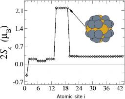
FeNi alloys are widely used magnetic materials. Surprisingly experiments have shown that the magnetic moment per atom in FeNi clusters is much lower than that of the bulk alloy of the same composition [1]. Using a Stoner-like tight-binding model, including spin-orbit coupling, we have calculated the magnetic properties of fcc FexNi1-x clusters (x<0.6) containing up to about 300 atoms for several compositions and three types of chemical order: random and core-shell structures with either Ni or Fe cores [2]. The results show that only the latter type of order is compatible with the observed reduction of moment which can be explained by the existence of an anti-ferromagnetic order in the fcc Fe core (Fig.1)
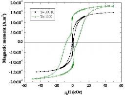
The discovery of the giant magnetoresistance (GMR) effects by Baibich et al. in Fe/Cr ferromagnetic multilayers provoked an important research effort and created the field of spintronics. The total current flow is described as the result of two independent conduction channels with electrons of different spin. Spin-dependent resistance is usually described by two scattering phenomena: one arising from the bulk of the magnetic layers and the other from the diffusion of electrons at the interface between magnetic layers and non-magnetic spacer layers. Two approaches have been used for a theoretical description of the GMR in current in plane (CIP) configuration, the “semiclassical” one deduced from the pioneering work of Fuchs and Sondheimer and the quantum-mechanical Kubo formalism. In the semiclassical approach, spin-dependent bulk resistivities and spin-dependent interfacial resistivities are taken into account. Thus in this model the spin-dependent interfacial resistivity is treated by introducing the proportions of electrons transmitted, specularly reflected, or diffusely scattered from the interfaces. In CIP magnetoresistance experiments, bulk and interface scattering contributions are usually not separable. The work of C. Gatel et al. [1] was to analyze the spin dependence of electron reflection and to experimentally examine the CIP-GMR effect which is only produced by the spin-dependent interfacial reflection. In this framework, the team of the CEMES has grown by sputtering epitaxial trilayers on α-Al2O3(0001) substrates consisting of two ferromagnetic insulating (FI) layers with different coercive fields: CoFe2O4(111) and Fe3O4(111) (which becomes an insulator below the Verwey transition) separated by a non-magnetic metallic (M) Au or Pt layer. The interfacial flatness and the high structural quality of these CoFe2O4/(Au or Pt)/Fe3O4 trilayers have been evidenced by X-ray reflectivity, X-ray diffraction and TEM [1]. One problem that had to be addressed was the 2D epitaxial growth of a thin and continuous metallic layer onto an oxide surface [2]. Figure 1 shows the magnetic hysteresis loops curves obtained in an Au-based system for different temperatures. Magnetic loops exhibit the butterfly-like shape corresponding to the separate switching of the two magnetic layers (first reversal due to Fe3O4).
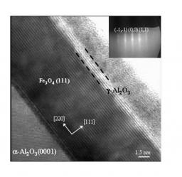
At first we have studied the growth of fully epitaxial Fe3O4(111)/γ-Al2O3(111) bilayers to be included in a MTJ. Epitaxial growth by molecular beam epitaxy (MBE) of a γ-Al2O3 ultra-thin layer (a few nanometers) on top of a magnetite electrode was achieved by evaporation of metallic aluminium from a Knudsen effusion cell under atomic oxygen. The RHEED diffraction patterns (inset of figure 1) recording during the growth demonstrated the two-dimensional growth mode of Al2O3. In situ Auger electron spectroscopy (AES) and X-ray photoelectron spectroscopy (XPS) measurements (Fe 2p and Al 2p core levels) have also been performed in order to check the oxidation state of Fe at the Fe3O4/Al2O3 interface and the full homogeneous oxidation of aluminium. In appropriate growth conditions (Al flux, atomic oxygen pressure), we were able to obtain a stoichiometric Fe3O4/Al2O3 interface [1,2]. The magnetic properties of these stoichiometric bilayers, obtained by VSM magnetometry and XMCD analyses (not shown here), exhibited the same magnetic behavior (remanence, coercivity, Verwey transition, magnetic moment) as the corresponding uncovered Fe3O4 layers. The HRTEM cross section in figure 1 confirmed the very good epitaxy of the Fe3O4(111)/γ-Al2O3(111) system. Finally, the insulating properties of the γ-Al2O3(111) ultra-thin layers have been measured using a conductive tip AFM (Coll. UMR CNRS/Thales) validating the tunnel barriers properties [1,2]. No pinholes have been detected, demonstrating that the Fe3O4 layer is entirely covered by a 1.5 nm thick Al2O3 layer.
The magnetic properties (spin and orbital magnetic moments, magneto-crystalline anisotropy energy (MAE)) of nanoparticles, thin films and wires have recently attracted a lot of attention due to their potential applications mainly in the Information Technology sector.
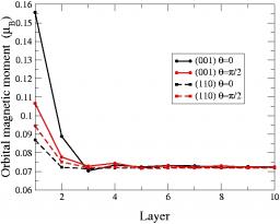
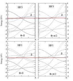
We have carried out a systematic study of the magnetic properties of iron in the tight-binding approximation including s, p, and d valence atomic orbitals taking into account spin polarisation using a Stoner-like model and in the presence of spin-orbit coupling[1]. The validity of the model has first been established by studying in details the magnetic properties of the bcc and fcc bulk phases and comparing the results to those of ab-initio calculations using the PWscf code. This model has then been applied to investigate the (110) and (001) bcc surfaces. The corresponding electronic structures and magnetic moments are very similar to those obtained from ab-initio codes. In addition we have studied the variation of the component of the orbital magnetic moment on the spin quantisation axis as a function of depth, revealing a significant enhancement in the first two layers, especially for the (001) surface (see Fig.1).
Spin electronics is an emerging science which aims at using the spin of the conduction electrons in electronic devices. In a near future, the fundamental mechanisms of spin transport will be affected by some physical limits linked to a further size reduction towards the nanometer scale. It is thus fundamental to understand these limits and more generally the physics of magnetism and transport in reduced dimensions.
Metal-metal nanocontacts are crucial in many areas, but have been poorly investigated from the point of view of local magnetism. This is a very appealing research domain, since local magnetism will greatly influence the (ballistic) conductance across a nanocontact. The break junction technique is a tool that allows the creation of stable (several hours) atomic contacts, which consists in breaking a material in a controlled manner by bending it until eventually a single atom contact appears between the two surfaces. Once a stable configuration is obtained the resistance can be measured as a function of an applied magnetic field. Michel Viret (CEA, SPEC) showed that in magnetic materials such as Fe, Co or Ni, one can obtain large magneto-resistive effects [1].
Guillaume MOUROT , Elisabeth BOUCHAUD
Coll: Stéphane MOREL, Gérard VALENTIN (Laboratoire LRBB, Université de Bordeaux, France)
C. Guerra Amaro, F. Célarié, Daniel BONAMY
Coll. Krishnaswamy Ravi-Chandar, University of Texas, Austin, USA,
D. Dalmas, UMR CNRS/Saint-Gobain, Aubervilliers
While continuum theory has allowed the determination (at least numerically) of the energy flux into the crack tip process zone for any dynamically growing crack (crack growth velocity comparable to sound velocity), efforts to relate this energy flux to the response of the crack have been only partially successful. While interacting with the material microstructure, dynamically growing cracks result in the release of elastic waves not taken into account in the theory in the absence of their precise knowledge.
Cindy Lynn ROUNTREE, Elisabeth BOUCHAUD
Coll: Mehdi TALAMALI, Damien VANDEMBROUCQ, (UMR CNRS/Saint-Gobain, Aubervilliers)
Stéphane ROUX (LMT, ENS-Cachan/CNRS-UMR 8535/Université Paris VI)
Rajiv KALIA (University of Southern California, Los Angeles, USA)
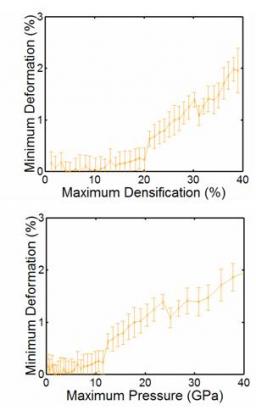
In order to understand the origin and nature of irreversible deformations in silica glass, we performed MD simulations of amorphous silica systems which are subjected to (1) a cyclic loading and unloading of the hydrostatic pressure and (2) a shearing force.
Alexandre MARCHENKO, Daniel BONAMY, Elisabeth BOUCHAUD, Denis FICHOU
Understanding the basic mechanisms that govern materials failure still represents a major challenge. It involves the material structure at small time and length scales through plastic deformation and damage, release of fluctuating elastic waves, and chemical processes. Understanding these phenomena calls for time-resolved observations and measurements of the fracture events at an atomic scale.
Cindy Lynn ROUNTREE, Silke PRADES, Daniel BONAMY, Davy DALMAS, Claude GUILLOT, Elisabeth BOUCHAUD
Coll. with Rajiv KALIA (University of Southern California, Los Angeles, USA)
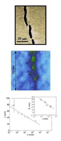
Fracture of pure silica, a “minimal” elastic material has been explored both experimentally and through numerical simulations. In both cases, the crack was shown to progress through the growth and coalescence of damage cavities ahead of the front. This mechanism was shown to be responsible for small scales non linear elastic behaviour both for ultraslow stress corrosion and dynamic fracture.
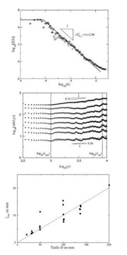
1.2.1. – Fracture mechanism
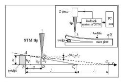
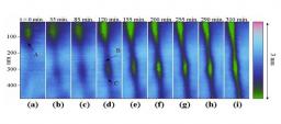
Stress corrosion ultraslow (average crack velocity ranging from 1 to 100 pm/s) mode I cracks in pure amorphous silica were followed with an Atomic Force Microscope (AFM) /1/, revealing the nucleation, growth and coalescence of damage cavities (see Fig. 1).
Laurent PONSON, Silke PRADES, Daniel BONAMY, Elisabeth BOUCHAUD, Claude GUILLOT
Laurent PONSON, Daniel BONAMY, Elisabeth BOUCHAUD, Claude GUILLOT,
Coll: Harold AURADOU and Jean-Pierre HULIN (Laboratoire FAST, Université d’Orsay, France),
Guillaume MOUROT and Stéphane MOREL (Laboratoire LRBB, Université de Bordeaux, France)
Philippe VIE (Laboratoire LMSGC, Laboratoire Central des Ponts & Chaussées, France)
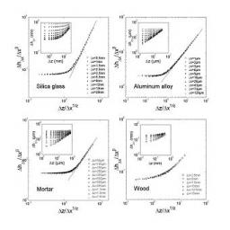
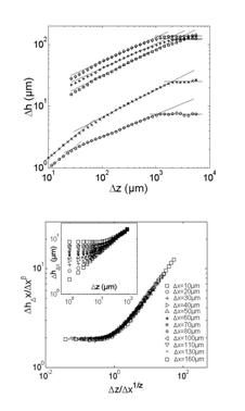
It was shown that a complete description of the statistical scaling properties of fracture surfaces in heterogeneous materials call for the use of the two-dimensional (2D) height-height correlation function /1/. This function was observed to exhibit anisotropic scaling properties similar to the Family-Viseck scaling predicted in interface growth models, characterized by three critical exponents ζ=0.75, β =0.6 and Z= ζ/β=1.2 independent to some extent of the considered material, the loading condition, and the crack growth velocity.
Daniel BONAMY,
Coll. : Mathieu RENOUF (LaMCoS, INSA de Lyon, Villeurbannes)
Frédéric DUBOIS, Pierre ALART (LMGC, Université Montpellier 2)
Bérengère DUBRULLE, Francois DAVIAUD (Groupe Instabilité & Turbulence, CEA/SPEC)
Pierre-Henri CHAVANIS (LPT, Université Paul Sabatier, Toulouse)
Fe3O4 is a very attractive material for applications involving spin-dependent transport at room temperature as this ferromagnetic oxide has a high Curie temperature (Tc= 858 K) and is predicted to be half-metallic. However, the potential applications of Fe3O4 layers in devices relies on the assumption that the magnetic and transport properties in the thin films are similar to those in the bulk material. Several studies have shown that the magnetic behaviour, resistivity, and magnetoresistance strongly deviate from the bulk due to the presence of antiphase boundaries (APBs) in the films. An APB is a stacking fault in the iron cation sublattice which can produce a new magnetic ordering and new magnetic couplings across the APBs. The aim of this section is to analyze rigorously the relationships between the APB density and the anomalous magnetic and magnetotransport properties observed in thin films. Epitaxial Fe3O4(111) thin films of thickness varying from 5 nm to 50 nm were deposited on a-Al2O3(0001) substrates by atomic oxygen plasma-assisted molecular beam epitaxy (MBE). The real time evolution of the film growth was monitored by reflection high-energy electron diffraction (RHEED) in order to verify the high crystalline quality. In addition, in situ X-ray photoemission spectroscopy (XPS), X-ray diffraction, high resolution transmission electron microscopy (HRTEM) measurements and plane view analyses were performed to characterize the structural and chemical properties of the magnetite films of all thicknesses. Figure 1 presents the dark-field images in plane view of Fe3O4 layers of varying thickness. These images qualitatively demonstrate the effect of the film thickness on antiphase domain size, i.e. the decrease in domain size with decreasing film thickness. In order to more quantitatively analyze the evolution of the antiphase domain size as a function of the film thickness, we have shown, in agreement with the work of Eerenstein et al. [1], that this average domain size varies as t1/2, where t is the film thickness. The thickness dependence of the APBs density could be derived from the antiphase domain size and varies as t-1/2 [2], [3]. This direct relationship between film thickness and APBs density has been used to study the influence of such structural defects on magnetic and magnetotransport properties observed in thin films.
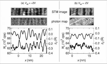
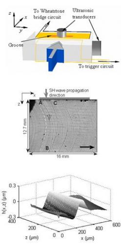
In the late 80's, near field microscopies got rich by a new technique when it has appeared that photons are emitted from the biased (V) tunnel junction (tip-surface) of a scanning tunneling microscope (STM). Soon, after the first evidence of the phenomena, contrast in the photon yield versus local morphology of the surface was reported. Its deep origin was a wide matter of debate during the last years.
Before our experiment, variation of the surface plasmon was the selected interpretation. In order to make a decisive experiment, we proposed to explore the photon emission from the simplest possible system: a gold tip in front on a (111) Au surface. The surface exhibits the usual reconstruction with small corrugation not larger than 0.01-0.03 nm, depending on the tip quality. A high correlated contrast of the photon rate, is mainly observed for V>0.
1Groupe Matière Condensée et Matériaux, UMR-CNRS 6626, Université de Rennes 1, 35042 Rennes, France
2 Laboratoire d’Optronique, FOTON, UMR-CNRS 6082, 22302 Lannion, France
3 Laboratoire Léon Brillouin (CEA-CNRS), CEA . Saclay, 91191 Gif-sur-Yvette Cedex
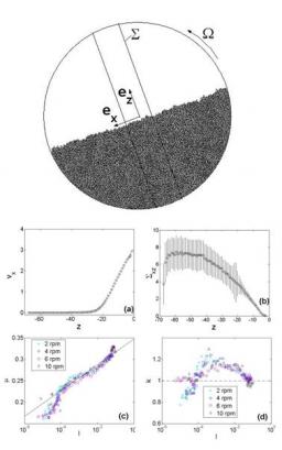
Anisotropic quenched disorder effects on a liquid crystal confined into nanochannels
Intense experimental and theoretical efforts have focused on quenched disorder effects in condensed matter as they bring about some most challenging questions of modern statistical physics. Most universal features of quenched disorder effects can be envisaged in the frame of random field theories. From this standpoint, liquid-crystals (LC) confined in random porous materials are definitively recognized as paradigm systems, which allows one to address experimentally general questions on phase transitions, critical scaling and non-ergodicity in the presence of quenched random fields. (More...)

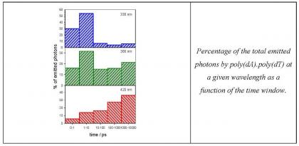
Polymeric and oligomeric DNA helices, poly(dAdT)·poly(dAdT) and (dAdT)10·(dAdT)10, composed of 200–400 and 20 adenine–thymine base pairs, respectively, are studied by fluorescence upconversion. Fluorescence decays, anisotropy decays and time-resolved spectra, obtained for this alternating base sequence, are compared with those determined previously for the homopolymeric sequence (dA)n·(dT)n. It is shown that identical fluorescence decays may correspond to quite different anisotropy decays and vice versa, both varying with the emission wavelength, the base sequence and the duplex size. Our observations cannot be explained in terms of monomer and excimer emission exclusively, as concluded in the past on the basis of steady-state measurements. Excitons also contribute to the fluorescence. These are rapidly trapped by excimers, characterized by long-lived weak emission.
The study of excited states and energy transfer in DNA double helices has recently gained new interest connected to the development of computational techniques and that of femtosecond spectroscopy. The present article points out contentious questions regarding the nature of the excited states and the occurrence of energy transfer and shows how they are currently approached. Using as example the polymer poly(dA)·poly(dT), composed of about 2000 adenine–thymine pairs, a model is proposed on the basis of time-resolved measurements (fluorescence decays, fluorescence anisotropy decays and fluorescence spectra, obtained with femtosecond resolution), associated to steady-state spectra. According to this qualitative model, excitation at 267 nm populates excited states that are delocalized over a few bases (excitons). Ultrafast internal conversion directs the excited state population to the lower part of the exciton band giving rise to fluorescence. Questions needing further investigations, both theoretical and experimental, are underlined with particular emphasis on delicate points related to the complexity and the plasticity of these systems.

Excited-State Relaxation Dynamics in DNA bases in the Gas-Phase
Time-resolved photoelectron and photoion fragmentation spectroscopy study of 9-methyladenine and its hydrates: a contribution to the understanding of the ultrafast radiationless decay of excited DNA bases
Canuel, C.; Elhanine, M.; Mons, M.; Piuzzi, F.; Tardivel, B.; Dimicoli, I.
Phys. Chem. Chem. Phys. 2006, 8, 3978 (PCCP Hot Paper)
Near-UV Resonant Two-Photon Ionization Spectroscopy of Gas Phase Guanine: Evidence for the Observation of Three Rare Tautomers
Mons, M.; Piuzzi, F.; Dimicoli, I.; Gorb, L.; Leszczynski, J.
J. Phys. Chem. A 2006, 110, 10921
Theoretical study of the ground and excited states of Guanine, 7 methyl Guanine, and 9 methyl Guanine: Comparison with experiment
Cerny, J.; Spirko, V.; Mons, M.; Hobza, P.; Nachtigallova, D.
Phys. Chem. Chem. Phys. 2006, 8, 3059
Excited states dynamics of DNA and RNA bases : Characterisation of a step-wise deactivation pathway in the gas phase
Canuel, C.; Mons, M.; Piuzzi, F.; Tardivel, B.; Dimicoli, I.; Elhanine, M.
J. Chem. Phys. 2005, 122, 074316
Tautomer contribution's to the near UV spectrum of guanine: towards a refined picture for the spectroscopy of purine molecules;
Chin, W.; Mons, M.; Dimicoli, I.; Piuzzi, F.; Tardivel, B.; Elhanine, M.
Eur. Phys. J. D 2002 20, 347
Ultraviolet spectroscopy and tautomerism of the DNA base guanine and its hydrate formed in a supersonic jet;
Piuzzi, F.; Mons, M.; Dimicoli, I.; Tardivel, B.; Zhao, Q.
Chem. Phys. 2001 270, 205
Spin electronics is an emerging science which aims at using the spin of the conduction electrons in electronic devices. In a near future, the fundamental mechanisms of spin transport will be affected by some physical limits linked to a further size reduction towards the nanometer scale. It is thus fundamental to understand these limits and more generally the physics of magnetism and transport in reduced dimensions.
Metal-metal nanocontacts are crucial in many areas, but have been poorly investigated from the point of view of local magnetism. This is a very appealing research domain, since local magnetism will greatly influence the (ballistic) conductance across a nanocontact. The break junction technique is a tool that allows the creation of stable (several hours) atomic contacts, which consists in breaking a material in a controlled manner by bending it until eventually a single atom contact appears between the two surfaces. Once a stable configuration is obtained the resistance can be measured as a function of an applied magnetic field. Michel Viret (CEA, SPEC) showed that in magnetic materials such as Fe, Co or Ni, one can obtain large magneto-resistive effects [1].
