


Fig. 1 : Structure of a nano-hybrid solar cell
Most solar cells industrially produced are currently based on silicon wafers (93.5 %). As a result, the price of photovoltaic modules is very high (5.6 €/Wp at its lowest in 2004) and is still expected to increase, due to a fast growing demand and a shortage in silicon production. Moreover, single-crystal silicon solar cells, which have a power conversion efficiency of more than 20 %, are heavy and fragile, which prevents them from being used for mobile applications.
Several concepts have been developed to tackle these problems. Inorganic thin film devices (based for example on amorphous silicon or CuInGaSe2) have reached efficiencies above 12 % and enter commercial stage. Organic solar cells are on the other hand expected to show lower production costs and easier integration on flexible substrates. Yet they still have low efficiencies (around 5 % at best) and suffer from short lifetimes as compared to inorganic devices.
Nanostructured materials are considered one of the best ways to improve the efficiency of organic and hybrid solar cells. Indeed, devices based on such materials have an increased interface area and a reduced average distance from one point to an interface. As the separation of charge carriers occurs at interfaces, such structures enhance it, and thus lead to an increase in the photocurrent. Bulk heterojunctions between polymers and inorganic nanoparticles lead to efficiencies of 1.8 % (with MDMO-PPV and branched CdSe nanoparticles). Devices, where nanostructured materials are directly grown on the substrate, would additionally bring an electrically continuous path from the active interface to the electrodes.[1]
The project aims at demonstrating the relevance of this approach by making devices (Fig. 2) based on silicon nanowires directly grown on a transparent conductive oxide, and poly(3-hexylthiophene), which shows one of the highest hole mobility among semi-conducting polymers (0.1 cm2.V-1.s-1).
This work has been divided into several steps :
• Study of the model case made of flat thin films of amorphous silicon and P3HT;
• Development of a method to grow silicon nanowires on ITO at low temperatures with control on their size and distribution (in cooperation with the LPICM, Ecole Polytechnique)
• Surface modification on the silicon nanowires to improve the contact with the polymer;
• Characterization of the photovoltaic performances of the device.
Cells based on flat thin films of amorphous silicon and P3HT have been made. They show a high rectification ratio, a power conversion efficiency up to 1.6 % and we demonstrated that the separation of charge carriers occurs at the interface between silicon and P3HT. [2] The silicon layer was grown by PECVD (Plasma Enhanced Chemical Vapor Deposition) and the polymer was spin-coated under nitrogen atmosphere before the top metal electrodes are deposited.
Yet the efficiency is limited by the interface between the top metal electrode and P3HT. It appears that the band alignment strongly depends on how much the polymer is doped by oxygen and on the conditions in which the metal electrodes (Au or Pd) are evaporated. To tackle the second problem, a method to deposit an intermediate layer of PEDOT : PSS has been developed.
Silicon nanowires have been grown on ITO and ZnO by thermal CVD (Chemical Vapor Deposition). Silane (SiH4) has been used as precursor gas, and two metal catalysts have been tested: gold and copper. Metals are first evaporated on the substrates and form small islands when the latter is heated, due to different thermal dilatation coefficients. The growth is thought to occur through the VLS (Vapor-Solid-Liquid) mechanism. At a deposition temperature of 540 °C, straight nanowires with an average diameter ranging from 30 to 60 nm and an average apparent length of 100 to 500 nm have been obtained. As ITO is a polycrystalline material, the orientation of the wires appears to be random.
Work is currently in progress to better control the growth of the nanowires, and especially to understand the role and the evolution of the metal catalyst, the relation between the initial thickness of the metal layer, the size of the droplets after annealing and the size of the nanowires.
Contact:
REFERENCES :
(1) Zardo, I.; Yu, L.; Conesa-Boj, S.; Estradé, S.; Alet, P.-J.; Rössler, J.; Frimmer, M.; Roca i Cabarrocas, P.; Peiró, F.; Arbiol, J.; Morante, J. R.; Fontcuberta i Morral, A.; Gallium assisted plasma enhanced chemical vapor deposition of silicon nanowires; Nanotechnology 2009, 20, 155602.
(2) Yu, L.; Alet, P.-J.; Picardi, G.; Roca i Cabarrocas, P.; An In-Plane Solid-Liquid-Solid Growth Mode for Self-Avoiding Lateral Silicon Nanowires; Phys. Rev. Lett. 2009, 102, 125501
(3) Yu, L.; Alet, P.-J.; Picardi, G.; Maurin, I.; Roca i Cabarrocas, P.; Synthesis, morphology and compositional evolution of silicon nanowires directly grown on SnO2 substrates; Nanotechnology 2008, 19, 485605.
(4) Alet, P.-J.; Yu, L.; Patriarche, G.; Palacin, S.; Roca i Cabarrocas, P.; In situ generation of indium catalysts to grow crystalline silicon nanowires at low temperature on ITO; J. Mater. Chem. 2008, 18, 5187 - 5189.
(5) Alet, P.-J.; Roca i Cabaroccas, P.; Palacin, S.; Patent FR0851817, 20/03/2008.
(6) Alet, P.-J.; Palacin, S.; Roca i Cabarrocas, P.; Low-temperature growth of nano-structured silicon thin films on ITO initiated by metal catalysts; Thin Solid Films 2008, 517, 6405-6408.
(7) Alet, P.-J.; Eude, L.; Palacin, S.; Roca i Cabarrocas, P.; Transition from thin gold layers to nano-islands on TCO for catalyzing the growth of one-dimensional nanostructures; Physica Status Solidi A 2008, 205, 1429-1434.
(8) Alet, P.-J.; Palacin, S.; Roca i Cabarrocas, P.; Kalache, B.; Firon, M.; de Bettignies, R.; Hybrid Solar Cells Based on Thin-Film Silicon and P3HT; Eur. Phys. J. Appl. Phys. 2007, 36, 231-234.
(9) Firon, M.; Drevillon, B.; Fontcuberta i Morral, A.; Palacin, S.; Roca i Cabaroccas, P. Patent EP1774605, 21/07/2004
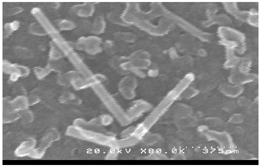
Fig. 2 : Silicon nanowires grown on ZnO using Au as a catalyst
• ![]() Électronique et optique du futur › Matériaux pour l'électronique et l'optique - Electronique organique et moléculaire
Électronique et optique du futur › Matériaux pour l'électronique et l'optique - Electronique organique et moléculaire
• Service de Physique et Chimie des Surfaces et des Interfaces • Laboratory of Physics and Chemistry of Surfaces and Interfaces
• Laboratoire Innovation, Chimie des Surfaces Et Nanosciences- LCSI (LICSEN-LCSI) • Laboratory of Chemistry of Surfaces and Interfaces (LCSI)
