


Pages scientifiques 2014
Contact : Ludovic Tortech (NIMBE/LICSEN & UPMC)
Des capteurs extrêmement sensibles nés des recherches en spintronique et capables de détecter des champs magnétiques ultra-faibles sont déjà sur le marché. Des développements importants sont attendus dans le futur grâce, d’une part, à des avancées technologiques et, d’autre part, à la mise en œuvre de nouveaux concepts comme le transfert de spin ou l’utilisation de matériaux multiferroïques. Néanmoins, malgré ces développements et le transfert réussi entre recherche académique et utilisation « grand public », des questions fondamentales restent en suspens. Parmi ces questions, on peut citer le problème de l’adaptation des dispositifs de la spintronique aux matériaux semi-conducteurs, la compréhension et le contrôle du signe de la polarisation en spin dans les dispositifs et, pour aller au-delà de ce qui existe, la création de nouveaux systèmes basés sur des concepts nouveaux où le transport de spin peut être modulé et éventuellement contrôlé par une perturbation extérieure (champ électrique, pression ou lumière).
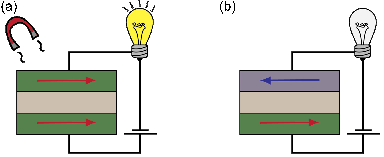
FIG. 1 : Représentation schématique d’un dispositif GMR composé d’une couche FM bloquée (vert), d’une couche libre magnétique (vert ou violet), et d’une couche séparatrice métallique. (a) Le dispositif est dans le mode parallèle et le courant polarisé en spin circule; (b) le dispositif est dans le mode antiparallèle et le courant ne circule pas.
La vanne de spin, qui est le dispositif de base de la spintronique, est constituée de deux électrodes ferromagnétiques (FM) séparées par un métal non magnétique d’épaisseur nanométrique. Selon l’orientation des aimantations des électrodes (parallèle ou antiparallèle), pilotée à l’aide d’un champ magnétique extérieur, la résistance électrique de la jonction varie. Cette une variation importante de la résistance électrique en fonction du champ magnétique est la "magnétorésistance géante" (GMR) découverte par A. Fert et P. Grünberg en 1988. Dans une telle jonction, il est possible de remplacer l’espaceur métallique par un isolant non magnétique d’épaisseur nanométrique définissant ainsi une jonction tunnel magnétique (JTM). On obtient dans ce cas un effet de magnétorésistance tunnel (TMR) avec une amplitude qui peut atteindre plusieurs centaines de pourcents à température ambiante. Néanmoins, en fonction de la nature chimique de la barrière tunnel, de son épaisseur et de sa morphologie, l’amplitude/signe de la TMR peut changer drastiquement. Pour comprendre les effets observés, il est nécessaire de contrôler l’interaction entre l’électrode et l’espaceur et notamment la structure de l’interface, comme cela a pu être fait dans le cas de la barrière tunnel de MgO.
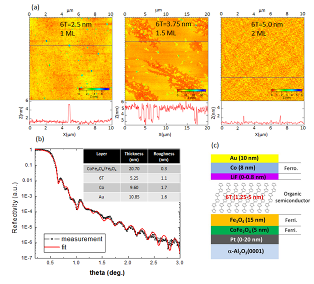
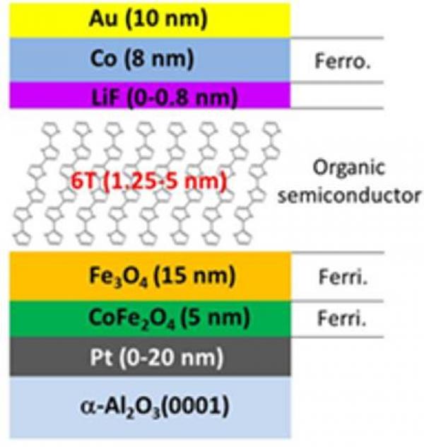
FIG. 2: De haut en bas : images AFM d’un film mince de sexi-thiophène sur Fe3O4, graphe de réflectivité des neutrons (épaisseur de couches), et structure des composants étudiés.
Au laboratoire nous étudions en collaboration avec Jean-Baptiste Moussy (IRAMIS/SPEC) de nouvelles structures basées sur l’utilisation de films minces de semi-conducteurs organiques. Nous avons ainsi mis en évidence récemment qu’il est possible de modifier la nature du couplage d’échange magnétique dans les JTMs Fe3O4/6T/Co (ou 6T désigne le sexithiophène) notamment lorsque le film de sexithiophène est particulièrement mince (une mono-couche) [1].
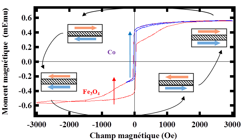
FIG. 3: Cycle d’hystérèse de mesure du moment magnétique d’une couche mince organique entre 2 électrodes magnétiques et leur orientation magnétique individuelle.
PhD thesis of: Hugo CASADEMONT
Contacts: Bruno JOUSSELME & Vincent DERYCKE
MoS2 Transistors with Ultrathin and Robust Organic Gate Dielectric
Dielectric films with nanometer thickness play a central role in the performances of field effect transistors (FETs). In this article, a new class of organic gate dielectric based on the electrochemical grafting of diazonium salts on metallic electrodes is investigated. The versatile diazonium salt strategy is a local and room-temperature process that provides robustness and performances. Moreover, this process produces ultrathin (4-8 nm) and smooth films. To prove their efficiency as gate dielectric, they were integrated in MoS2-FETs gate stacks. The devices display excellent switching behavior for reduced gate bias swing (down to 1V) and suppressed hysteresis thank to the highly hydrophobic nature of the fluorinated grafted film. Furthermore, the devices exhibit steep subthreshold slopes (as low as 110 mV/decade), demonstrating excellent gate coupling.
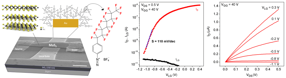
We are presently extending this study to CVD-based monolayer MoS2 and to flexible devices.
Référence :
[1] Electrografted Fluorinated Organic Ultrathin Film as Efficient Gate Dielectric in MoS2 Transistors
H. Casademont, L. Fillaud, X. Lefevre, B. Jousselme, V. Derycke, J. Phys. Chem. C (2016), in press - link

Dans le cadre de la thèse de: Aurélie Paquirissamy
Contacts: Géraldine Carrot (Nimbe/LICSEN) & Jean-Philippe Renault (Nimbe/LIONS)
Nano-objets polymères et hybrides sous irradiation
Les nano-objets polymères ou hybrides sont utilisés sous irradiation dans de nombreux domaines : lithographie, radiostérilisation, radiosensibilisation. Cependant, il existe peu d’études sur l’interaction de ces objets nanométriques avec les rayonnements. Dans le présent travail, nous avons développé deux familles de nano-objets afin d’étudier leurs comportements sous irradiation. La première est à base de copolymères à blocs à la fois hydrophiles et hydrophobes, pouvant s’auto-organiser dans l’eau (micelles, vésicules). Les objets à base de polyéthylène glycol (PEG) varient de par la nature de leur polymère hydrophobe (polyméthacrylate, polysulfone) et leur sensibilité aux rayonnements ionisants. Les nanoparticules métalliques étant connues pour augmenter l’effet de l’irradiation, nous avons également synthétisé des nanoparticules d’or greffées de chaînes polymères. Après irradiation dans l’eau, on observe une diminution de la taille de ces objets qui s’explique à la fois par des coupures en bout de chaînes (analyses par chromatographie d’exclusion stérique - CES) et par du dégreffage de chaînes polymères sur la nanoparticule (mesures par diffusion de neutrons aux petits angles – DNPA, effectuées au LLB). En présence de cellules cancéreuses, ces nanoparticules d’or greffées ont montré leur efficacité en termes de radiosensibilisation. Lorsqu’un médicament anticancéreux comme la doxorubicine est greffé sur les chaînes polymères, l’activité biologique est conservée après couplage et irradiation. A long terme, on peut donc envisager de combiner activité radiosensibilisante et transport de molécules chimiothérapeutiques dans le même nano-objet.
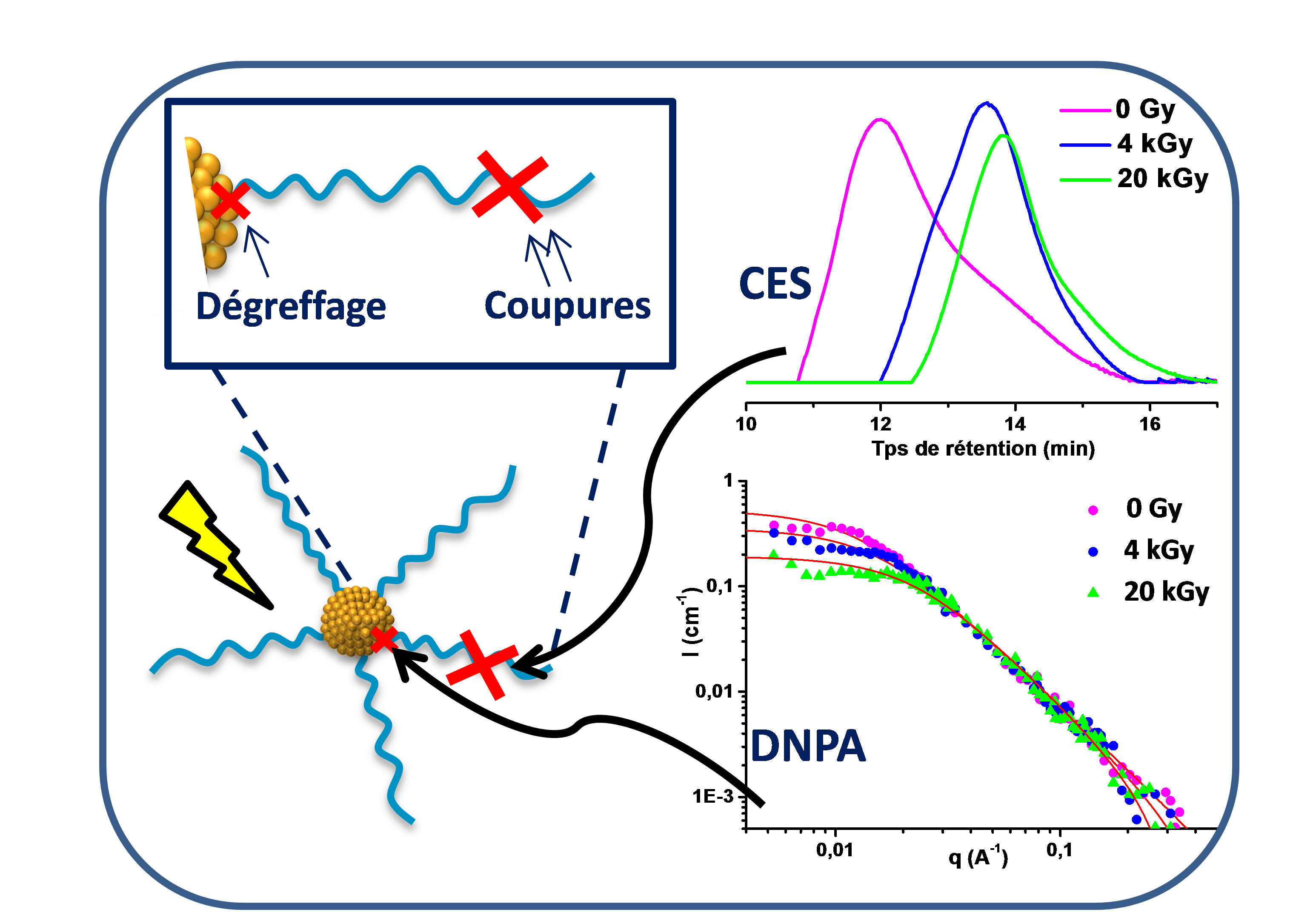
Les analyses par chromatographie d’exclusion stérique (en haut à droite) montrent, en fonction de la dose d’irradiation, un déplacement du signal vers les temps de rétention plus long, correspondant à des masses molaires plus faibles des chaînes dégreffées. En DNPA, la diminution de l’intensité du signal à q=0 (en bas à droite) montre une baisse de la masse totale des objets.
Multiferroic compounds are materials which show several order parameters including for instance ferroelectricity and magnetism. The coupling between these two orders is an important property called magnetoelectric coupling leading to exciting potential applications in information technology and sensors. Bismuth ferrite (BiFeO3) is the only multiferroic with both ordering temperatures way above room temperature, but unfortunately, it is antiferromagnetic. Nevertheless, one can imaging coupling it with ferromagnets, which are more easily measurable, to make a working device.
Another alternative lies in using the properties of topological defects like domain walls (DW), which have their own interesting properties. In particular, these objects can have a magnetic moment as well as interesting photo-electric properties. They can also be manipulated with an electrical field and as such, they offer potential for non-volatile storage, logic or optoelectronic devices.
One PhD project (Camille Blouzon) supported by the ANR “Multidolls” is to study bismuth ferrite DW properties, including photovoltaic and magnetic… A wide range of characterization technics as synchrotron radiation, neutron scattering, and original homemade experimental setups will be used.
Electric field switching of Rashba splitting using ferroelectric polarization
The ambition of our work is to control spin-orbit coupling in an emerging class of spintronics materials, such as topological insulators and their parent compounds, deposited on thin films ferroelectric (FE) substrate (Figs. 1, 2 and 3). One of the most interesting and useful features of FE materials is the strong coupling of the polarization with elastic strain that can be switched by an external electric field. The remnant polarization in a FE should provide a robust and reproducible control of the Rashba-type electron band spin splitting in a 2D system and therefore potentially of spin transport properties.
Experimental and theoretical studies within the project will be closely matched to obtain valuable information on spin polarisation and contribute to providing a framework for new type of applications in spintronics.
|
|
|
|
|
|
|
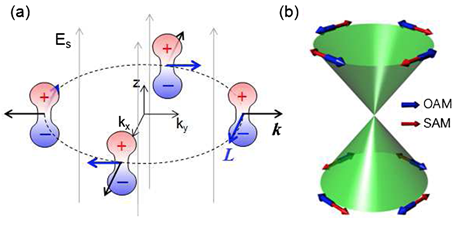
Figure 1: a) Interaction of the electric dipole moment and surface electric field Es, and resulting alignment of the orbital angular momentum (OAM). |
|
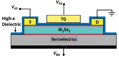
Figure 2: Scheme of a back-gated/top-gated device. The top and bottom TI surface states are indicated by red lines. |
|
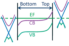
Figure 3: Schematic variation of the band structure along the vertical direction, showing the bulk conduction (purple) and valence (green) bands bending. The TI states bands (light blue) can be shifted by application of a gate voltage. |
Topological Insulators
Topological insulators (TI) are new states of quantum matter in which surface states residing in the bulk insulating gap of such systems are protected by time-reversal symmetry ([HAS10], [Qi11]). The electronic band structure of these materials includes characteristic conical features at high-symmetry points within the Brillouin zone. Electrons in the vicinity of a cone exhibit linear dispersion and are expected to behave like massless Dirac fermions confined within a two-dimensional plane (Fig. 4).
The transport properties of a topological insulator are closely related to the two-dimensional (2D) integer quantum Hall effect, which also has unique edge states. These electronic states are insensitive to disorder because there are no states available for backscattering. They were originally predicted to exist in graphene [Kan05, Ber06]. Graphene is made out of carbon, which is a light element with a weak spin-orbit interaction. Clearly, a better place to look for this physics would be in materials with strong spin-orbit interactions, made from heavy elements near the bottom of the Periodic Table.
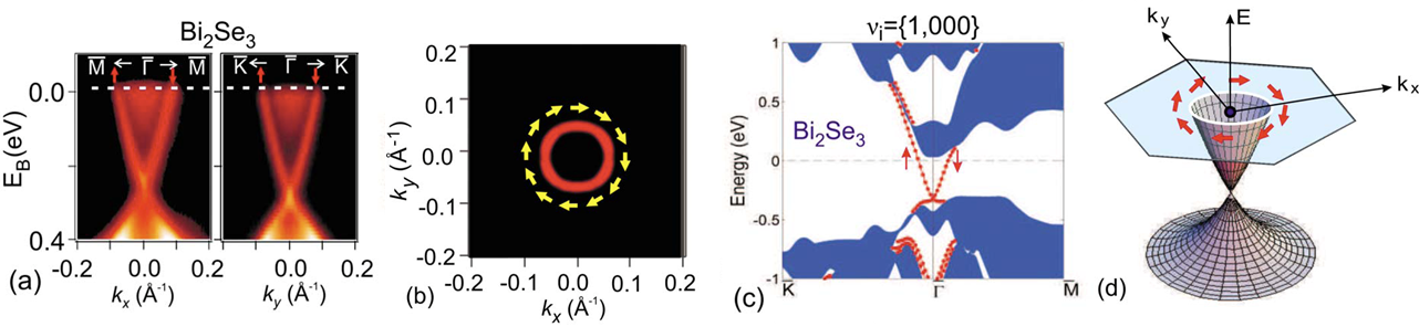
Figure 4: Spin-momentum locked helical surface Dirac fermions are hallmark signatures of topological insulators. a) ARPES data for Bi2Se3 reveal surface electronic states with a single spin-polarized Dirac cone. b) The surface Fermi surface exhibits a chiral left-handed spin texture. c) Surface electronic structure of Bi2Se3 computed in the local-density approximation. The shaded regions describe bulk states, and the lines are surface states. d) Schematic of the spin-polarized surface-state dispersion in Bi2X3 (1;000) topological insulators.
From: [Has10]
Topological Insulators: Thin films
Whereas the surfaces of bulk topological insulators provide a promising basis for spintronics application, thin films are more relevant for actual device architecture. Effort has been made to reduce the thickness of known bulk topological insulators. The choice of available materials is thus substantially broadened. However, the usable film thickness has a natural lower limit, below which the two film boundaries may be coupled by quantum tunnelling, so that a small, thickness-dependent gap opens up at the Dirac point, cutting off the spin conduction.
Thin film parent compound of topological insulators
The requirement of fine-tuning the thickness makes the experimental fabrication of 2D topological insulators rather difficult. Therefore, it is desirable to search for new materials or new schemes to obtain a 2D topological insulator. The Bi(111) film on a suitable substrate actually represents a special interesting class of films having an intermediate inter-bilayer (BL) coupling strength that may have a significant influence on the topological property [Liu11]. It should be noted that the substrate may have additional effects on the electronic structure and hence the topological properties of Bi films, which are of central interest for these studies.
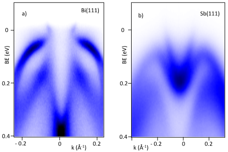
Figure 5: ARPES spectra of: a) (111) face of a Bi monocrystal (12 ML) prepared on a InAs(111)-A face; b) (111) face of a Sb monocrystal prepared on a Bi(111) buffer layer shown in a).
We have extensive experience with thin layer growth. Bi growth is epitaxial and a Bi monocrystal of very high quality is obtained after depositing several monolayers (Fig. 5a). The band dispersion fits well with literature data on Bi single crystals [Hof06, Hir06]. On top of Bi(111) we were able to prepare high quality Sb(111) monocrystals (Fig. 5b). The Sb(111) and the Bi(111) surfaces have a hexagonal structure; their lattice constants are 4.30 and 4.54 Å, respectively; so the lattice mismatch is ~5% for Sb grown on a Bi buffer layer.
Theoretical description
This part of the work will be done in close collaboration with our colleagues from Ludwigs-Maximilians-Universität, Munich, Germany. The interpretation of the spin dependent band structure, as observed in ARPES, will be supported by ab-initio Korringa-Kohn-Rostoker (KKR) electronic structure calculations which account for all aspects of the investigated TIs: spin-orbit coupling without approximations by a fully relativistic approach, interdiffusion and disorder by means of the coherent potential approximation (CPA) and correlations by the dynamical mean field theory (DMFT). For this the layer dependent spin texture, as well as the spin and orbital resolved Bloch-spectral function will be determined. The measured ARPES spectra will be complemented by calculations on the basis of the one-step model of photoemission that accounts for all relevant aspects like matrix elements and final state effects, in a state-of-the art way. [Min11b, Min11, Min13].
Understanding the formation of nanoparticles in water at room temperature is a major challenge, both to tackle the mechanisms of mineral growth in biological systems, and to synthesise efficiently nanomaterials. However, the growth mechanisms usually invoked sometimes fail dramatically to describe reality, especially the final size, the crystalline quality and rate of production of the nanocrystals. Progress in this area are slow because of the great difficulty in observing the intermediate steps between the solution before reaction, and the construction of the first nanocrystal. A group of researchers from the IRAMIS/NIMBE, the Laboratory of Condensed Matter Physics at the École Polytechnique and the Université Pierre-et-Marie-Curie has managed this feat by using in particular the SOLEIL synchrotron radiation. Their observations allowed to propose a formation scenario which is unusual, but consistent with reality, and probably very generic. These results have been recently published in ACS Nano.
Since the beginning of the years 2000, more and more examples of functional amyloid fibers have been discovered in bacteria and fungi as well as in the mammals’ realm[1-2]. Very recently, a study on about forty peptide hormones has demonstrated that those were stored inside pituitary secretory granules under the form of amyloid fibers[3].
Beyond the structural biology question, we are especially interested in these molecules because we think they might be appropriate models to tackle broader issues like biomimetic self-assembly and amyloid formation – amyloid understood as “beta-sheet rich assembly”.
Indeed, peptides are generally small and easily synthesizable molecules that, if our hypothesis is right, will form reversible amyloid-like assemblies whose structure and assembly mechanism will be carefully studied.
Le cycle géologique des éléments volatils est régi par des transferts entre les réservoirs de la surface (ex. atmosphère, océans) et les réservoirs profonds (ex. manteau terrestre). Ces transferts s’opèrent via le volcanisme et via le recyclage de la croûte terrestre dans les zones de subduction.
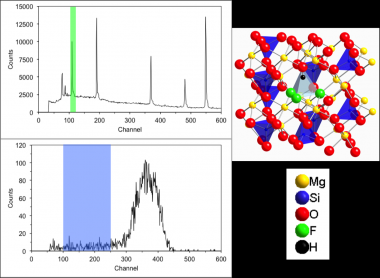
Ainsi il est important de déterminer la capacité d’insertion d’un élément tel le fluor dans des minéraux hôtes présents dans le manteau. Dans le cadre d’une collaboration entre l’UPMC, le CEA, l’université d’Edinburgh et l’université of Western Ontario, l’étude de la co-incorporation du fluor et de l’eau dans la forstérite, minéral représentatif du manteau supérieur (jusqu’à 400 km de profondeur environ) a été entreprise. Ces minéraux ont été synthétisés dans des presses piston cylindre afin de reproduire les conditions de pression et de température du manteau supérieur.
En combinant deux techniques analytiques disponibles à la microsonde nucléaire du LEEL, il a été possible de doser l’eau et le fluor, éléments difficiles à mesurer dans ce type d’échantillons. Le fluor est quantifié par la réaction nucléaire 19F(p,p’γ)19F, l’eau (via l’hydrogène) par la technique ERDA 1H(α,p)4He.
Les résultats ont montré qu’il existe bien un lien entre l’incorporation du fluor et celle de l’eau. Le mécanisme d’incorporation du fluor, qui fait intervenir des défauts mixtes hydroxyle-fluorure, a par ailleurs pu être élucidé en combinant modélisation moléculaire ab initio et observations par spectroscopie infrarouge. Ces résultats suggèrent que les minéraux majeurs du manteau terrestre peuvent accommoder la totalité du fluor transitant par ce réservoir et que les cycles de l’eau et du fluor sont liés.
Clumped fluoride-hydroxyl defects in forsterite: Implications for the upper-mantle
C. Crépisson, M. Blanchard, H. Bureau, C. Sanloup, A. C. Withers, H. Khodja, S. Surblé, C. Raepsaet, K. Béneut, C. Leroy, P. Giura, E. Balan, Earth and Planetary Science Letters 390 (2014) 287.
Since the beginning of the years 2000, more and more examples of functional amyloid fibers have been discovered in bacteria and fungi as well as in the mammals’ realm[1-2]. Very recently, a study on about forty peptide hormones has demonstrated that those were stored inside pituitary secretory granules under the form of amyloid fibers[3].
Beyond the structural biology question, we are especially interested in these molecules because we think they might be appropriate models to tackle broader issues like biomimetic self-assembly and amyloid formation – amyloid understood as “beta-sheet rich assembly”.
Indeed, peptides are generally small and easily synthesizable molecules that, if our hypothesis is right, will form reversible amyloid-like assemblies whose structure and assembly mechanism will be carefully studied.
Electric field switching of Rashba splitting using ferroelectric polarization
The ambition of our work is to control spin-orbit coupling in an emerging class of spintronics materials, such as topological insulators and their parent compounds, deposited on thin films ferroelectric (FE) substrate (Figs. 1, 2 and 3). One of the most interesting and useful features of FE materials is the strong coupling of the polarization with elastic strain that can be switched by an external electric field. The remnant polarization in a FE should provide a robust and reproducible control of the Rashba-type electron band spin splitting in a 2D system and therefore potentially of spin transport properties.
Experimental and theoretical studies within the project will be closely matched to obtain valuable information on spin polarisation and contribute to providing a framework for new type of applications in spintronics.
|
|
|
|
|
|
|
Figure 1: a) Interaction of the electric dipole moment and surface electric field Es, and resulting alignment of the orbital angular momentum (OAM). |
|
Figure 2: Scheme of a back-gated/top-gated device. The top and bottom TI surface states are indicated by red lines. |
|
Figure 3: Schematic variation of the band structure along the vertical direction, showing the bulk conduction (purple) and valence (green) bands bending. The TI states bands (light blue) can be shifted by application of a gate voltage. |
Topological Insulators
Topological insulators (TI) are new states of quantum matter in which surface states residing in the bulk insulating gap of such systems are protected by time-reversal symmetry ([HAS10], [Qi11]). The electronic band structure of these materials includes characteristic conical features at high-symmetry points within the Brillouin zone. Electrons in the vicinity of a cone exhibit linear dispersion and are expected to behave like massless Dirac fermions confined within a two-dimensional plane (Fig. 4).
The transport properties of a topological insulator are closely related to the two-dimensional (2D) integer quantum Hall effect, which also has unique edge states. These electronic states are insensitive to disorder because there are no states available for backscattering. They were originally predicted to exist in graphene [Kan05, Ber06]. Graphene is made out of carbon, which is a light element with a weak spin-orbit interaction. Clearly, a better place to look for this physics would be in materials with strong spin-orbit interactions, made from heavy elements near the bottom of the Periodic Table.
Figure 4: Spin-momentum locked helical surface Dirac fermions are hallmark signatures of topological insulators. a) ARPES data for Bi2Se3 reveal surface electronic states with a single spin-polarized Dirac cone. b) The surface Fermi surface exhibits a chiral left-handed spin texture. c) Surface electronic structure of Bi2Se3 computed in the local-density approximation. The shaded regions describe bulk states, and the lines are surface states. d) Schematic of the spin-polarized surface-state dispersion in Bi2X3 (1;000) topological insulators.
From: [Has10]
Topological Insulators: Thin films
Whereas the surfaces of bulk topological insulators provide a promising basis for spintronics application, thin films are more relevant for actual device architecture. Effort has been made to reduce the thickness of known bulk topological insulators. The choice of available materials is thus substantially broadened. However, the usable film thickness has a natural lower limit, below which the two film boundaries may be coupled by quantum tunnelling, so that a small, thickness-dependent gap opens up at the Dirac point, cutting off the spin conduction.
Thin film parent compound of topological insulators
The requirement of fine-tuning the thickness makes the experimental fabrication of 2D topological insulators rather difficult. Therefore, it is desirable to search for new materials or new schemes to obtain a 2D topological insulator. The Bi(111) film on a suitable substrate actually represents a special interesting class of films having an intermediate inter-bilayer (BL) coupling strength that may have a significant influence on the topological property [Liu11]. It should be noted that the substrate may have additional effects on the electronic structure and hence the topological properties of Bi films, which are of central interest for these studies.
Figure 5: ARPES spectra of: a) (111) face of a Bi monocrystal (12 ML) prepared on a InAs(111)-A face; b) (111) face of a Sb monocrystal prepared on a Bi(111) buffer layer shown in a).
We have extensive experience with thin layer growth. Bi growth is epitaxial and a Bi monocrystal of very high quality is obtained after depositing several monolayers (Fig. 5a). The band dispersion fits well with literature data on Bi single crystals [Hof06, Hir06]. On top of Bi(111) we were able to prepare high quality Sb(111) monocrystals (Fig. 5b). The Sb(111) and the Bi(111) surfaces have a hexagonal structure; their lattice constants are 4.30 and 4.54 Å, respectively; so the lattice mismatch is ~5% for Sb grown on a Bi buffer layer.
Theoretical description
This part of the work will be done in close collaboration with our colleagues from Ludwigs-Maximilians-Universität, Munich, Germany. The interpretation of the spin dependent band structure, as observed in ARPES, will be supported by ab-initio Korringa-Kohn-Rostoker (KKR) electronic structure calculations which account for all aspects of the investigated TIs: spin-orbit coupling without approximations by a fully relativistic approach, interdiffusion and disorder by means of the coherent potential approximation (CPA) and correlations by the dynamical mean field theory (DMFT). For this the layer dependent spin texture, as well as the spin and orbital resolved Bloch-spectral function will be determined. The measured ARPES spectra will be complemented by calculations on the basis of the one-step model of photoemission that accounts for all relevant aspects like matrix elements and final state effects, in a state-of-the art way. [Min11b, Min11, Min13].
