


Patents 2006
Numéro d'identification: WO/2006/042839 (Lien OMPI, Fichier PDF associé)
Numéro d'identification CEA: BD 1587
Date de dépôt: 18-10-2004
Année de publication: 27-04-2006
Procédé et appareil de mesures de champ magnétique au moyen d'un capteur magnétorésistant
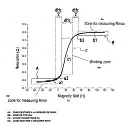
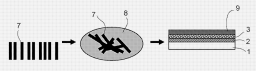
L'invention concerne un dispositif permettant de mesurer un champ magnétique au moyen d'un capteur magnétorésistant et comprenant au moins un capteur magnétorésistant (5), un module (50) permettant de mesurer la résistance dudit capteur (5), un module générateur (40, 6) permettant de générer un champ magnétique supplémentaire dans l'espace renfermant le capteur magnétorésistant (5) et une unité de commande (60) permettant, dans un premier temps, de commander de manière sélective le module générateur (40, 6) afin qu'il applique une impulsion de champ magnétique supplémentaire possédant une première valeur dotée d'une première polarité soit positive, soit négative et une amplitude suffisante pour saturer le capteur magnétorésistant (5), puis permettant de commander de manière sélective la mesure de la résistance du capteur magnétorésistant (5) par le module (50), aux fins de mesure de la résistance.
A method and apparatus for magnetic field measurements using a magnetoresistive sensor
(lien WIPO)
The device for measuring magnetic field by using a magnetoresistive sensor comprises at least one magnetoresistive sensor (5) , a module (50) for measuring the resistance of the magnetoresistive sensor (5) , a generator module (40, 6) for generating an additional magnetic field in the space containing the magnetoresistive sensor (5) , and a control unit (60) firstly for selectively controlling the generator module (40, 6) to apply an additional magnetic field pulse possessing a first value with first polarity that is positive or negative and magnitude that is sufficient to saturate the magnetoresistive sensor (5) , and secondly for selectively controlling measurement of the resistance of the magnetoresistive sensor (5) by the module (50) for measuring resistance.
Contacts: C. Fermon et M Pannetier-Lecoeur
Numéro d'identification: WO/2006/029649 (Lien OMPI)
Numéro d'identification CEA : BD1567
Date de dépôt : 15-09-2004
Année de publication: 23-03-2006
Oscillateur pour hyperfréquences accordé avec un mince film ferromagnétique
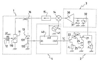
L'invention concerne un oscillateur accordé pour hyperfréquences, faisant appel à un résonateur à mince film ferromagnétique, qui comprend: a) un résonateur hyperfréquences (1) comportant une plaque de résonance (110) à mince film ferromagnétique, comme un cristal YIG en forme de disque, placé sur un circuit intégré hyperfréquences (11), tel qu'un résonateur sur feuille à demi-longueur d'ondes; b) un moyen de champ magnétique de polarisation (12) pour appliquer un champ magnétique de polarisation à la plaque de résonance (110) à film ferromagnétique mince; c) un élément actif pour assurer l'oscillation (21), un élément de retour réactif (24) et une charge (23, 25) régulée par les propriétés hyperfréquences de la plaque de résonance (110) à film ferromagnétique mince, à travers une boucle de rétroaction de charge (4) et d) une boucle de rétroaction positive générale (3, 14, 15), connectée entre l'élément actif pour assurer l'oscillation (21) et le résonateur hyperfréquences (1) pour induire une oscillation soutenue à créer à une des résonances excitées par paramètres de la plaque de résonance (110) à film ferromagnétique mince.
Microwave oscillator tuned with a ferromagnetic thin film
(lien WIPO)
A microwave tuned oscillator utilizing a ferromagnetic thin film resonator comprises: a) a microwave resonator (1) comprising a ferromagnetic thin film resonance plate (110) such as a disc-shaped YIG crystal placed on a microwave integrated circuit (11), such as a half-wavelength strip-line resonator, b) bias magnetic field means (12) for applying a bias magnetic field perpendicular to the ferromagnetic thin film resonance plate (110), c) an active element for oscillation (21), a reactive feedback element (24) and a load (23, 25) controlled by the microwave properties of the ferromagnetic thin film resonance plate (110) through a load feedback loop (4), and d) an overall positive feedback loop (3, 14, 15) connected between the active element for oscillation (21) and the microwave resonator (1) to cause a sustained oscillation to build up at one of parametrically excited resonances of the ferromagnetic thin film resonance plate (110).
Contacts: O. Klein et V. Naletov
Numéro d'identification : WO/2006/018497 (Lien OMPI et fichier PDF associé)
Numéro d'identification CEA BD: 1574
Année de dépôt : 20-07-2004
Date de publication : 23-02-2006
Dispositif semiconducteur à nanotube ou nanofil, configurable optiquement
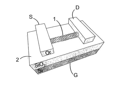
L'invention concerne un dispositif semiconducteur comprenant au moins un nanotube ou un nanofil, notamment de carbone, ainsi qu'au moins deux électrodes, caractérisé en ce qu'elles comportent au moins un nanotube ou un nanofil semiconducteur ayant au moins une région au moins en partie recouverte d'une couche de molécules ou de nanocristaux d'un matériau photo-sensible, une liaison électrique entre les deux électrodes étant réalisée par au moins un nanotube ou un nanofil semiconducteur.
Optically-configurable nanotube or nanowire semiconductor device
(WIPO link)
The invention relates to a semiconductor device comprising at least one nanotube or nanowire, such as a carbon nanotube or nanowire, as well as two electrodes. The invention is characterized in that the device comprises at least one semiconductor nanotube or nanowire having at least one region which is at least partially covered with at least one layer of molecules or nanocrystals made from at least one photo-sensitive material. According to the invention, an electrical connection is provided between the two electrodes by at least one nanotube, namely the semiconductor nanotube or nanowire, and optionally at least one other nanotube or nanowire.
Contact: J.P. Bourgoin
Numéro d'identification : WO/2006/011013 (Lien OMPI, Fichier PDF associé)
Numéro d'identification CEA : BD1555
Année de dépôt 16-07-2004
Année de publication: 22-02-2006
Dispositif de protection permettant de protéger un circuit contre une attaque mécanique et électromagnétique
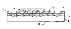
Pour protéger un circuit contre une attaque mécanique ou électromagnétique, un dispositif de protection active fixé au circuit comprend : au moins un générateur servant à générer un champ magnétique, au moins un capteur magnétique S1, S2, S3, S4 servant à mesurer une valeur du champ magnétique, un circuit d'intégrité connecté au(x) capteur(s) magnétique(s) S1, S2, S3, S4 et au circuit. Le circuit d'intégrité active une procédure de réaction dans le circuit si la valeur du champ magnétique mesurée par le capteur magnétique sort d'un domaine de valeurs qui est corrélé au champ magnétique généré.
An active protection device for protecting circuit against mechanical and electromagnetic attack.
(Lien WIPO)
For protecting a circuit against a mechanical or electromagnetic attack, an active protection device attached to the circuit comprises: - at least one generator for generating a magnetic field, - at least one magnetic sensor S1, S2, S3, S4 for measuring a value of the magnetic field, - an integrity circuit connected to the at least one magnetic sensor S1, S2, S3, S4 and to the circuit. The integrity circuit activates a reaction procedure in the circuit if the measured value of the magnetic field made by the magnetic sensor is out of a values domain, the values domain being correlated to the generated magnetic field.
Contact: C. Fermon
Numéro d’identification WO/2006/018575 (lien WIPO)
Numéro d’identification CEA BD 13190
Année de dépôt : 21.07.2005
Date de publication : 23.02.2006
Nanocomposite photoactif et son procede de fabrication
L'invention concerne un nanocomposite (3) photoactif comportant au moins un couple d'éléments semiconducteurs donneur-accepteur. L'un des éléments est formé de nanofils (7) dopés à structure sp3, et l'autre des éléments est un composé organique (8). Lesdits éléments sont supportés par un substrat (1 ) de dispositif. L'invention concerne aussi un procédé de fabrication. Selon un premier mode de réalisation, après leur croissance, les nanofils (7) sont prélevés, fonctionnalisés et sont solubilisés dans l'élément organique (8). Le mélange est déposé par enduction sur un substrat de dispositif. Selon un deuxième mode de réalisation, des nanofils (7) sont formés sur un substrat de croissance (5) qui est aussi le substrat de dispositif. L'élément organique (8) est associé aux nanofils (7) de façon à former une couche active (3). Un tel nanocomposite (3) photoactif permet la réalisation d'une cellule photovoltaïque.
Contact : Serge Palacin (SPCSI)
Photoactive nanocomposite and method for the production thereof (WIPO link)
The invention relates to a photoactive nanocomposite (3) comprising at least one pair of donor-acceptor semiconductor elements, wherein an element consists of a nanowires (7) doped with an sp3 structure and another element in embodied in the form of an organic compound (8). Said elements are carried by the substrate (1) of a device. A production method is also disclosed and consists, in a first embodiment, in picking, fonctionalising and solubilizing the grown nanowires in the organic element (8) and in depositing the mixture by coating on the device substrate. In the second embodiment, the nanowires (7) are formed on a growth substrate (5) which is embodied in the form of the device substrate. The organic element (8) is associated with the nanowires (7) in such a way that an active layer (3) is formed. The inventive photoactive nanocomposite makes it possible to produce a photovoltaic cell.
Contact: Serge Palacin (SPCSI)
