


|
Black phosphorus (BP) is a stack of monoatomic layers of phosphorus, bound together by Van der Waals forces. This 2d material is today attracting a great interest due to its widely tunable band gap, depending on the thickness of the material, the very high mobility of its carriers, for its application in field effect transistors (FETs), and the possible emergence of topologically protected states. It has been shown that electrostatic action or evaporation of alkali metals, as electron donors, can be successfully used for doping the PB from a semiconductor phase to a semi-metallic phase with Dirac cone transport channels (with linear dispersion). Experimentalists and theoreticians at the Laboratory for Irradiated Solids (LSI) have thus studied the excited electronic states of black phosphorus after deposition of an increasing dose of alkaline atoms. The FemtoARPES (angle-resolved photoemission) experimental device at the LSI was used to monitor the band gap closure with unprecedented accuracy. This engineering of the electronic band structure would enable the design of devices with improved and optimized electronic and optoelectronic functionality. |
Ultimate-thin layers of simple elements, from a monolayer to a few layers, such as graphene, silicene... or MX2 dichalcogenide of transition metal, are two-dimensional systems with very specific electronic properties, which are seeking to be exploited. The idea is to be able to customize the electronic band structure to allow the realization of fast original electronic devices or for optoelectronics.
Another of these systems is black phosphorus (BP) composed, like an ultra-thin film of graphite, of a few monoatomic layers of phosphorus only bound by Van der Waals forces. Recent theoretical studies suggest that its electronic states and gap width can be reversibly controlled by charge injection techniques. These results are an indication of the potential of the PB as a basic building block for functional devices based on original electronic transport mechanisms. A simple approach to follow the evolution of electron dispersion curves under the effect of charge injection is to combine the deposition of alkaline atoms, as electron donors, and the observation of the band structure by ARPES (angularly resolved photoemission spectroscopy).
The present study concerns the monitoring by Femto-ARPES of the evolution of the band structure of BP during the deposition of a thin layer of caesium or potassium. Such an alkaline layer induces the presence of a strong electric dipole on the surface which can modify the electronic structure of BP. Time-resolved ARPES (Femto-ARPES) is a powerful technique that uses a pump laser pulse (1.55 eV) followed by a probe pulse (6.3 eV) to populate and then probe by photoemission the conduction band states [1]. The technique allows to observe the dispersion curves of the electronic states and to measure the gap. It can be noted that the relatively high energy of the probe beam gives a sufficiently long escape length to the excited electrons to reliably observe the evolution of the buried valence band.
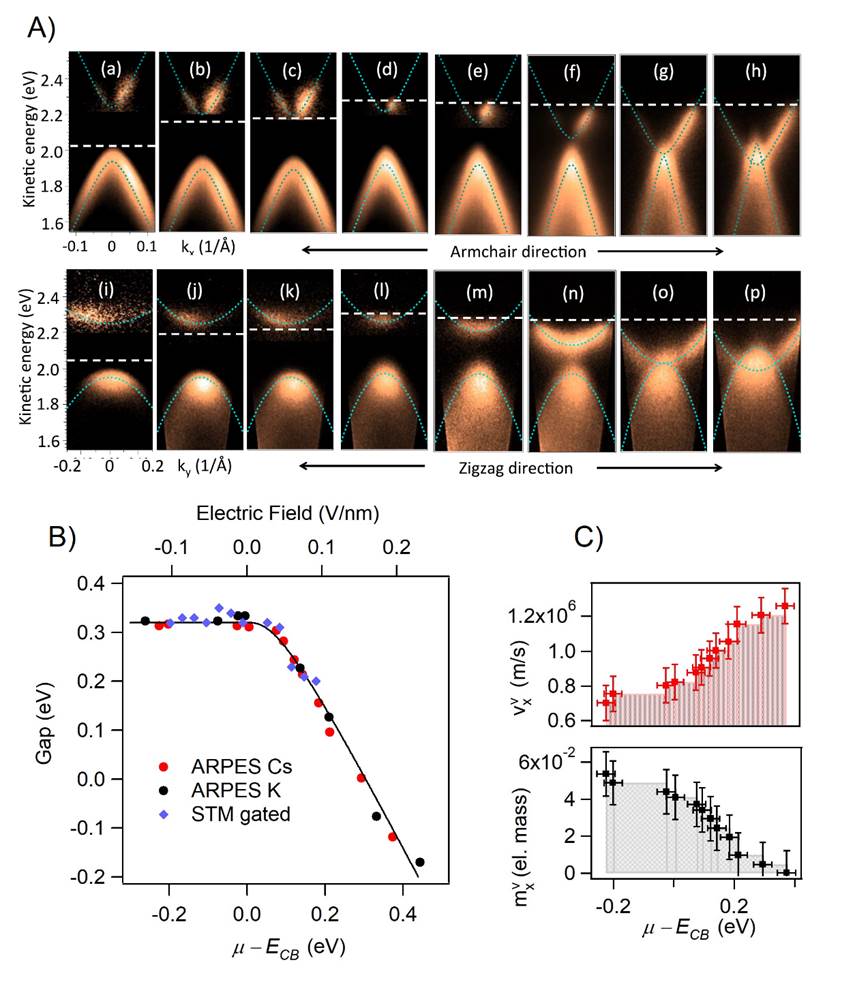
A) Time-resolved ARPES data of BP along the armchair direction, as function of surface doping. The dashed lines indicate the position of chemical potential μ.
B) Band gap at the surface of BP as function of surface doping by deposition of Cs atoms (red filled circles) and K atoms (black filled circles), respectively. The surface doping (bottom axis) is quantified by the difference between chemical potential μ and the minimum of the conduction band energy ECB. The solid line is a guide to the eye. As a term of comparison, the gap value (blue diamond) obtained by STM as function of polarizing field (top axis) is extracted from Ref. [3].
C) The fermi velocity (top) and effective mass (bottom) of the valence band along armchair direction and as function of doping level.
It is thus observed that during alkali deposition (i.e. by increasing the electronic doping) the gap monotonously narrows from the initial value of 0.32 eV for the bare sample, to zero for the largest cesium deposits [2]. Excellent agreement is obtained with STM measurements on a BP sample [3] (see Figure B). These data are also consistent with the results of density functional theory (DFT) calculations showing a steady decrease of the gap under potassium deposit. Finally, figure C shows that the "Fermi velocity" of the electrons is very high. In the high doping regime, the holes moving in the highly dispersive direction even acquire a band velocity higher than that of graphene on silicon carbide.
This study shows that the electronic structure of black phosphorus can be easily shaped by electron doping. Such electron structure tunability is also expected in the case of grid devices and suggests, as observed by alkali doping, that the mobility of excited electrons in the black phosphorus accumulation layer can be significantly increased in the presence of a high carrier density.
References:
[1] "Band Gap Renormalization, Carrier Multiplication, and Stark Broadening in Photoexcited Black Phosphorus” Z. Chen, J. Dong, E. Papalazarou, M. Marsi, C. Giorgetti, Z. Zhang, B. Tian, J.-P. Rueff, A. Taleb-Ibrahimi and L. Perfetti, Nano Lett. 19, 488 (2019).
[2] "Spectroscopy of buried states in black phosphorous with surface doping"
Z. Chen, J. Dong, C. Giorgetti, E. Papalazarou, M. Marsi, Z. Zhang, B. Tian, Q. Ma, Y. Cheng, J.-P. Rueff, A. Taleb-Ibrahimi, and L. Perfetti, Under review in "2D materials".
[3] " Gate-Tunable Giant Stark Effect in Few-Layer Black Phosphorus"
Y. Liu, Z. Qiu, A. Carvalho, Y. Bao, H. Xu, S. J. R. Tan, W. Liu, A. H. Castro Neto, K. P. Loh, J. Lu, Nano Lett. 17, 1970 (2017).
________________________________________
Contact CEA-IRAMIS: Luca Perfetti (Laboratoire de Solides Irradiés/ groupe Nouveaux Etats Electroniques)
Collaboration:
- Z. Chen, J. Dong, C. Giorgetti & L. Perfetti, Laboratoire des Solides Irradiés, CEA-IRAMIS, École Polytechnique, CNRS, Institut Polytechnique de Paris, F-91128 Palaiseau, France.
- A. Taleb & J.-P. Rueff: Synchrotron Soleil, L’Orme des Merisiers, Saint-Aubin BP 48 91192 Gif-sur-Yvette Cedex, France.
- E. Papalazarou & M. Marsi, Laboratoire de Physique des Solides, CNRS, Université Paris-Saclay, Université Paris-Sud, 91405 Orsay, France.
