


|
In optics, the possibility to confine light below its natural wavelength is hampered by the longstanding barrier of the diffraction limit. Surface plasmons are electromagnetic surface waves coupled to free electrons at metal dielectric interfaces. They offer a unique opportunity for scaling down photonic devices to the nanometre range. Experiments carried out in the SPCSI have investigated the differences between the spatial and spectral signatures of metallic nano-objects whether they are observed in far field (observed with our eyes in a classic optical microscope) or in near-field (observed at subwavelength scale using a photoemission electron microscope PEEM). This investigation brings important fundamental results in the plasmonics research field for the scaling down of photonic devices to the nanometre range. |
We have investigated the optical answer of gold nanostars synthesized by colloidal chemistry. They consist of a near-spherical core from which 5 to 8 sharp tips point outwards. The average tip to tip distance amounts to 120 nm - 150 nm. Three different microscopies have been used, namely :
- The low energy electron / photoemission electron microscopy LEEM / PEEM, allowing for high resolution near field mappings,
- The scanning electron microscopy SEM,
- The dark field microscopy DFM, allowing the spectral investigation of individual particles.
Under optical excitation objects smaller than the exciting wavelength exhibit remarkable absorption properties in relation to coherent collective oscillations of the charge carriers inside the particle. Spatially, these plasmon resonances translate into highly localized hot spots at the surface of the objects. Figure 1 displays the generic behavior of two different nanostars under optical excitation. Figures (a,d) correspond to the topographic signatures recorded by SEM. Figures (b,e) show the near field mappings of the corresponding objects at different wavelengths. Figures (c,f) are superpositions of both topographic and optical signatures providing clear evidence that the bright spots of high photoelectron emission intensity spatially coincide with locations of the tips of the nanostars.
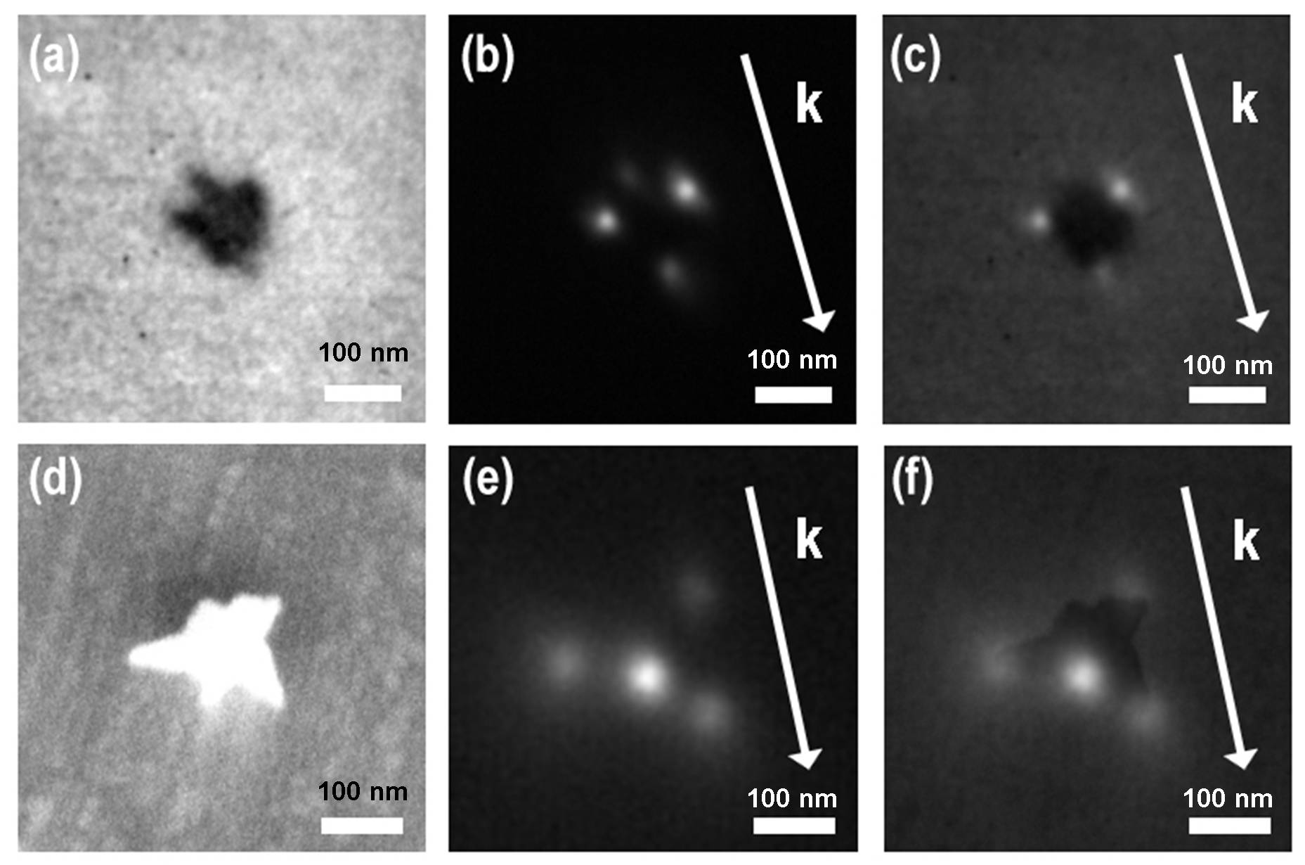
Figure 1.
- (a) LEEM image of a Au nanostar (nanostar I), electron kinetic energy 1.8 eV,
- (b) PEEM imaging of nanostar I under 730 nm laser excitation: composite image representing the sum of two PEEM images obtained under p-polarization and p + 40°- polarization, respectively,
- (c) Sum of (a) and (b),
- (d) SEM image of a Au nanostar (nanostar II),
- (e) PEEM imaging of nanostar II : composite image representing the sum of three PEEM images obtained with 860 nm excitation and p–42°-polarization, 780 nm excitation and p-polarization, and 860 nm excitation and p+48°-polarization, respectively.
- (f) Sum of (d) and (e).
For all PEEM images: grazing incidence of the laser at a = 73°, incident power density of ~125 MW/cm², the white arrow represents the k-vector of the laser light. The white scale bars represent 100 nm.
By adjusting both polarization and/or wavelength of the exciting beam, we can achieve the selective excitation of individual hotspots/tips in a single nanostar. A characteristic example is displayed in figure 2.a through d providing evidence that three of the four tips (of nanostar II) can be excited individually. From a careful comparison, spectrometric differences between near and far field signatures of the very same objects exists (peak positions). Size effects beyond the quasi static approximation (radiation damping, retardation of the exciting field) have been identified as the major processes affecting the peak positions of near- and far-field signatures. So, even for a 120 - 150 nm size object, size and shape effects beyond the quasi static approximation are of importance.
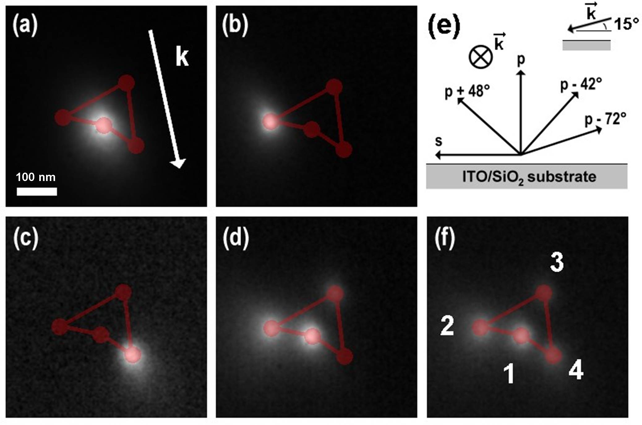
Figure 2. PEEM images of nanostar II under laser excitation
- (a) 860 nm wavelength p polarization,
- (b) 860 nm, p – 72° polarization,
- (c) 760 nm, p + 48° polarization,
- (d) 860 nm, p - 42° polarization.
- (e) PEEM polarization diagram.
- (f) nanostar II tip numbering. The superimposed red polygon indicates the relative positions of the photoemission hot spots. For all images: grazing incidence of the laser at a=73°, incident power density of ~125 MW/cm², the white arrow represents the k-vector of the laser light. The white scale bars represent 100 nm.
In conclusion, plasmonic hotspots in single gold nanostars are located at the tips and can be excited selectively by laser light as evidenced by photoelectron emission microscopy. Selectivity is achieved through wavelength and polarization of the excitation light. Comparing photoelectron emission intensity and dark-field scattering spectra of the same individual nanostars reveals both similarities and complementarities of the two techniques in terms of observable plasmon resonances, estimates of field enhancement, and sensitivity to absorption and scattering, respectively.
This investigation combining photoelectron emission, low energy electron, and scanning electron microscopies brings important fundamental results in plasmonics for the scaling down of photonic devices to the nanometre range.
Reference:
|
Selective excitation of individual plasmonic hotspots at the tips of single gold nanostars, |
 |
1Photonics and Optoelectronics Group, Department of Physics and CeNS, Ludwig-Maximilians Universität München, Amalienstr. 54, D-80799 München, Germany
2CEA, IRAMIS, Service de Physique et Chimie des Surfaces et Interfaces, F-91191 Gif sur Yvette, France
*Contact authors : and
