


Brevets 2002

Numéro d'identification : WO 2002/070148 (lien OMPI)
Numéro d'identification CEA : BD1356
Date de dépôt : 02-03-2001
Date de publication : 12-09-2002
Procédé de greffage organique localisé sans masque sur des portions conductrices ou semiconductrices de surfaces composites
Procédé de greffage localisé sans masque de molécules organiques susceptibles d'être électriquement activées, sur une surface composite comprenant des portions conductrices et/ou semi-conductrices, par mise en contact des molécules avec la surface. Le greffage est réalisé électrochimiquement en une seule étape sur des zones choisies, ces zones étant portées à un potentiel supérieur ou égal à un potentiel électrique seuil déterminé par rapport à une électrode de référence. Le potentiel électrique seuil est le potentiel au-delà duquel se produit le greffage des molécules organiques.
Method for mask-free localised organic grafting on conductive or semiconductive portions of composite surfaces(WIPO link)
The invention concerns a mask-free localised grafting of organic molecules capable of being electrically activated, on a composite surface comprising conductive and/or semiconductive portions, by contacting the organic molecules with the composite surface. The grafting is carried out electrochemically in one single step on specific selected zones of the conductive and/or semiconductive portions. These zones are brought to a potential higher than an electric potential threshold determined relatively to a reference electrode. the electric potential threshold is the potential beyond which the grafting of the organic molecules occurs.
Contact: S. Palacin
Numéro d'identification : WO 2002/085778 (Lien OMPI et Fichier PDF associé)
Numéro d'identification CEA BD1364
Année de dépôt : 19-04-2001
Date de publication : 31-10-2002
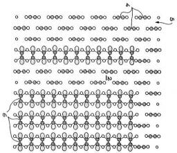
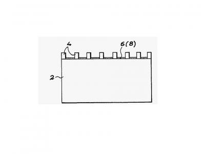
Procédé de fabrication de nanostructures unidimensionnelles et nanostructures obtenues par ce procédé
Procédé de fabrication de nanostructures unidimensionnelles et nanostructures obtenues par ce procédé. Selon l'invention, on forme des lignes atomiques parallèles (4), à la surface d'un substrat (2) de carbure de silicium, et on dépose sur cette surface une matière capable d'être adsorbée de façon sélective entre les lignes atomiques, sans l'être sur ces lignes atomiques, le dépôt de cette matière engendrant ainsi, entre les lignes atomiques, des bandes (6, 8) de cette matière. L'invention s'applique notamment à la fabrication de nanostructures possédant des bandes passivées ou métallisées.
Method for the production of one-dimensional nanostructures and nanostructures obtained according to said method (WIPO link)
According to the invention, parallel atomic lines (4) are formed on the surface of a silicon carbide substrate (2) and a material which can be selectively absorbed between the atomic lines without being absorbed on said atomic lines, is deposited on the surface, whereupon strips (6,8) of said material are created between said atomic lines. The invention is particularly suitable for use in the production of nanostructures having passivated or metalized strips.
Contact: P. Soukiassian
Numéro d'identification : WO 2002/086202 (Lien OMPI et fichier PDF associé)
Numéro d'identification CEA BD
Année de dépôt : 19-04-2001
Date de publication : 31-10-2002
Procédé de traitement de la surface d'un matériau semi-conducteur
Procédé de traitement de la surface d'un matériau semiconducteur, utilisant notamment l'hydrogène, et surface obtenue par ce procédé. Selon l'invention, on utilise par exemple l'hydrogène, on prépare la surface (S) pour qu'elle présente, à l'échelle atomique, une organisation contrôlée, et l'on hydrogène la surface ainsi préparée, la préparation et l'hydrogénation de la surface coopérant pour obtenir un état électrique prédéfini de la surface. L'invention trouve des applications, notamment en microélectronique, à la métallisation ou la passivation d'une surface semiconductrice.
Method for treating the surface of a semiconductor material (WIPO link)
The invention concerns a method for treating the surface of a semiconductor material, using in particular hydrogen, and the resulting surface. The invention is characterized in that it consists for example in using hydrogen, in preparing the surface (S) so that it has, on the atomic scale, controlled organization, and in hydrogenation of said prepared surface, the preparation and hydrogenation of the surface combining to obtain a predefined electric state of the surface. The invention is applicable, in particular in microelectronics, in metallization or passivation of a semiconductor surface.
Contact: P. Soukiassian