
Service de Physique de l'Etat Condensé

« Back to the Group page « Back to the Oxides page
Since these are collective electron phenomena, high resolution spectroscopy is necessary to untangle the electronic structure responsible for such phenomena. Thus, experimental tools which can contribute to a full understanding of the surface and near surface electronic and chemical structure are desirable, if possible with spatial resolution suitable for investigating individual domains or even phenomena localized at domain walls. Direct experimental data on the electronic structure of a FE next to an electrode is scarce due to the intrinsic difficulties of probing a buried interface. Photoelectron spectroscopy techniques are ideally suited since they reveal both electronic and chemical structure and the nanometric depth sensitivity may be tuned to the buried interface. To do these studies, the key is the combination of high quality sample preparation with state of the art experimental techniques to measure atomic, chemical and electronic structure.
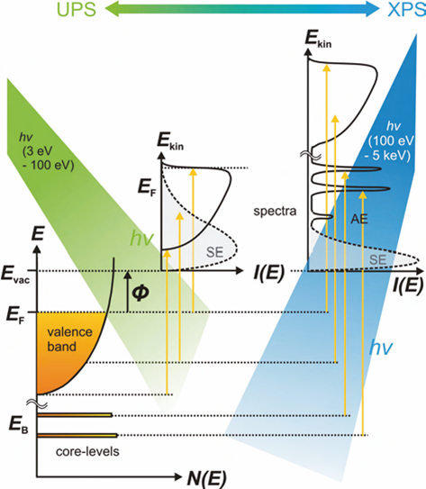
Photoelectron spectroscopy provides information on the initial state of the electron in the material, thus we can measure the chemical and electronic structure as well as the sample work function.
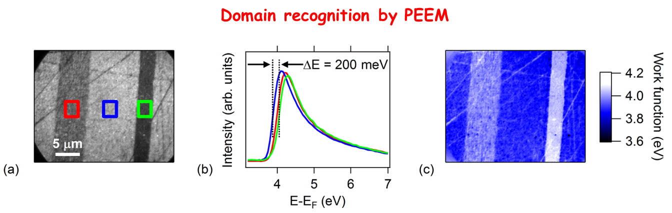
Photoelectron emission microscopy (PEEM) allows photoelectron spectroscopy with sub-micron spatial resolution. It can be used, for example, to perform domain polarization recognition at the surface of single crystal samples.
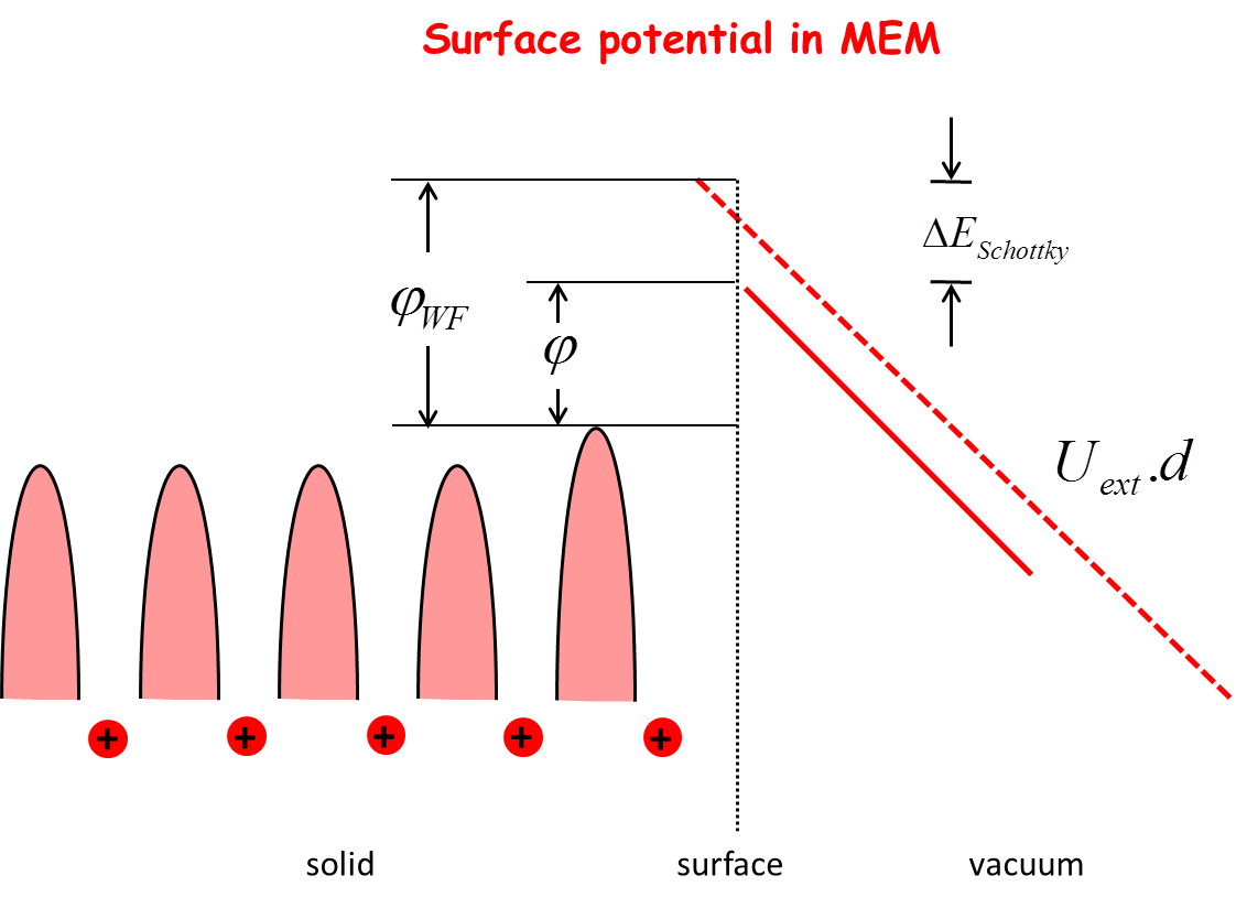
Low energy electron microscopy (LEEM) maps the surface electrostatic potential, a sort of complement to the work function mapping by PEEM.
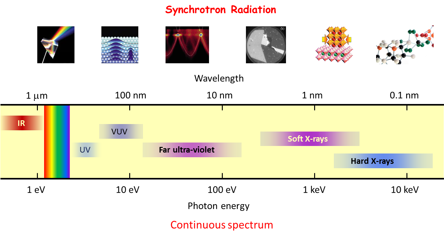
Synchrotron radiation broadens considerably the experimental possibilities of photoelectron spectroscopy thanks to the tunable, high intensity radiation.
