Service de Physique de l'Etat Condensé


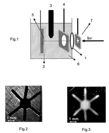
Cellule d'électrolyse utilisée dans le cadre de l'invention
Numéro d'identification : WO/2009/037311 (Lien OMPI, fichier PDF associé)
Numéro d'identification CEA BD 1759
Année de dépôt : 20-09-2007
Date de publication : 26-03-2009
Procédé d'électrogreffage localisé sur des substrats semi-conducteurs photosensibles
La présente invention concerne un procédé de préparation d'un film organique sur une zone sélectionnée à la surface d'un substrat semi-conducteur photosensible, comprenant les étapes suivantes : (i) mise en contact d'une solution liquide comprenant un primaire d'adhésion organique avec une zone sélectionnée; (ii) polarisation de la surface du substrat à un potentiel électrique plus cathodique que le potentiel de réduction du primaire d'adhésion mis en œuvre à l'étape (i); (iii) exposition de la zone sélectionnée à un rayonnement lumineux dont l'énergie est supérieure égale à celle du gap du semi-conducteur.
The present invention relates to a method of preparing an organic film on a selected area of the surface of a photosensitive semiconductor substrate, characterized by the following steps: (i) a liquid solution comprising one organic adhesion primer is brought into contact with one selected area; (ii) the surface of the substrate is biased with an electrical potential more cathodic than the reduction potential of the adhesion primer used in step (i); and (iii) the selected area is exposed to light radiation of energy at least equal to that of the bandgap of the semiconductor.
Contact: S. Palacin
• › De la molécule au matériau moléculaire
• ![]() Institut Rayonnement Matière de Saclay • IRAMIS: Saclay Institute of Matter and Radiation • Laboratory of Physics and Chemistry of Surfaces and Interfaces • Service de Physique et Chimie des Surfaces et des Interfaces
Institut Rayonnement Matière de Saclay • IRAMIS: Saclay Institute of Matter and Radiation • Laboratory of Physics and Chemistry of Surfaces and Interfaces • Service de Physique et Chimie des Surfaces et des Interfaces
• Laboratory of Chemistry of Surfaces and Interfaces (LCSI) • Laboratoire Innovation, Chimie des Surfaces Et Nanosciences- LCSI (LICSEN-LCSI)
