
Service de Physique de l'Etat Condensé

Numéro d’identification: WO/2016/196157 (lien OMPI)
Numéro d’identification CEA BD
Année de dépôt : 05-06-2015
Date de publication : 08-12-2016
Elément de magnétorésistance à vanne de spin à réponse améliorée aux champs magnétiques
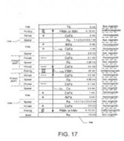
L’invention concerne un élément de magnétorésistance à vanne de spin qui comprend un nombre pair de structures de couches libres présentant un couplage ferromagnétique ou antiferromagnétique par rapport à des couches de laminage associées par des entretoises non magnétiques. Il peut présenter une configuration dans laquelle une moitié des structures de couches libres présente un couplage antiferromagnétique et l’autre moitié présente un couplage ferromagnétique par rapport à des couches laminées associées. Les couplages différents sont le résultat d’un nombre pair de couches d’entretoises différentes dont les épaisseurs respectives sont différentes..
Spin valve magnetoresistance element with improved response to magnetic fields (WIPO link)
A spin valve magnetoresistance element has an even number of free layer structures having ferromagnetic or antiferromagentic coupling with respecto to associated pinning layers via non-magnetic spacers. It may have a configuration in which one half of the free layer structures has an antiferromagnetic coupling and the other half has a ferromagnetic coupling with respect to associated pinned layers. The different couplings are the result of an even number different spacer layers having respective different thicknesses.
Contact: C. Fermon,
Numéro d’identification: WO/2015/105834 (lien WIPO)
Numéro d’identification CEA BD 15504
Année de dépôt : 09.01.2014
Date de publication : 16-07-2015
Elément magnétorésistif ayant une meilleure réponse aux champs magnétiques
Un élément magnétorésistif présente un agencement de piégeage comprenant deux couches de piégeage anti-ferromagnétiques, deux couches piégées et une couche libre. Une couche d'espacement entre l'une des deux couches de piégeage antiferromagnétiques et la couche libre présente un matériau sélectionné pour permettre un piégeage partiel régulable par l'une des deux couches de piégeage anti-ferromagnétiques.
Magnetoresistance element with improved response to magnetic fields (WIPO Link)
A magnetoresistance element has a pinning arrangement with two antiferromagnetic pinning layers, two pinned layers, and a free layer. A spacer layer between one of the two antiferromagnetic pinning layers and the free layer has a material selected to allow a controllable partial pinning by the one of the two antiferromagnetic pinning layers.
Contact: C. Fermon.

|
Numéro d’identification: WO/2015/105830 (lien OMPI) |
|
|
Numéro d’identification CEA BD 16020
Année de dépôt : 09.01.2014
Date de publication : 27.01.2015
Elément a effet de magnétorésistance a réponse améliorée aux champs magnétiques
L4invention concerne un élément à effet de magnétorésistance comportant un agencement à deux broches avec deux couches de brochage anti-ferromagnétiques, deux couches brochées, et une couche libre. Une couche d'écartement entre l'une des deux couches de brochage anti-ferromagnétiques et la couche libre comprend un matériau choisi pour permettre un brochage partiel contrôlable par une des deux couches de brochage anti-ferromagnétiques.
Magnetoresistance element with improved response to magnetic fields
A magnetoresistance element has a double pinned arrangement with two antiferromagnetic pinning layers, two pinned layers, and a free layer. A spacer layer between one of the two antiferromagnetic pinning layers and the free layer has a material selected to allow a controllable partial pinning by the one of the two antiferromagnetic pinning layers.
Contact: M. Pannetier-Lecoeur
Numéro d’identification : WO/2016/120557 (lien OMPI)
Numéro d’identification : CEA BD 15891
Année de dépôt : 28.01.2015
Date de publication : 04.08.2016
Dispositif de réhabilitation prothétique de la rétine
Un aspect de l'invention concerne un dispositif (10) de réhabilitation prothétique de la vision comportant : - un explant scléral (11) dont la forme est adaptée pour être au contact d'au moins une partie de la sclère d'un œil, et - au moins un inducteur (12) agencé sur l'expiant scléral (11)..
Device for prosthetic rehabilitation of the retina (WIPO link)
One aspect of the invention relates to a device (10) for prosthetic sight rehabilitation, which includes: a scleral explant (11) with a shape that is suitable for being in contact with at least one portion of the sclera of an eye; and at least one inducer (12) arranged on the scleral explant (11).
Contact: M. Pannetier-Lecoeur
 Numéro d’identification: WO/2016/124841 (lien OMPI)
Numéro d’identification CEA BD 15994
Année de dépôt : 03-02-2015
Date de publication : 11-08-2016
Procédé et dispositif de modulation de phase d'une onde porteuse et application à la détection de signaux numériques multi-niveaux codés en phase.
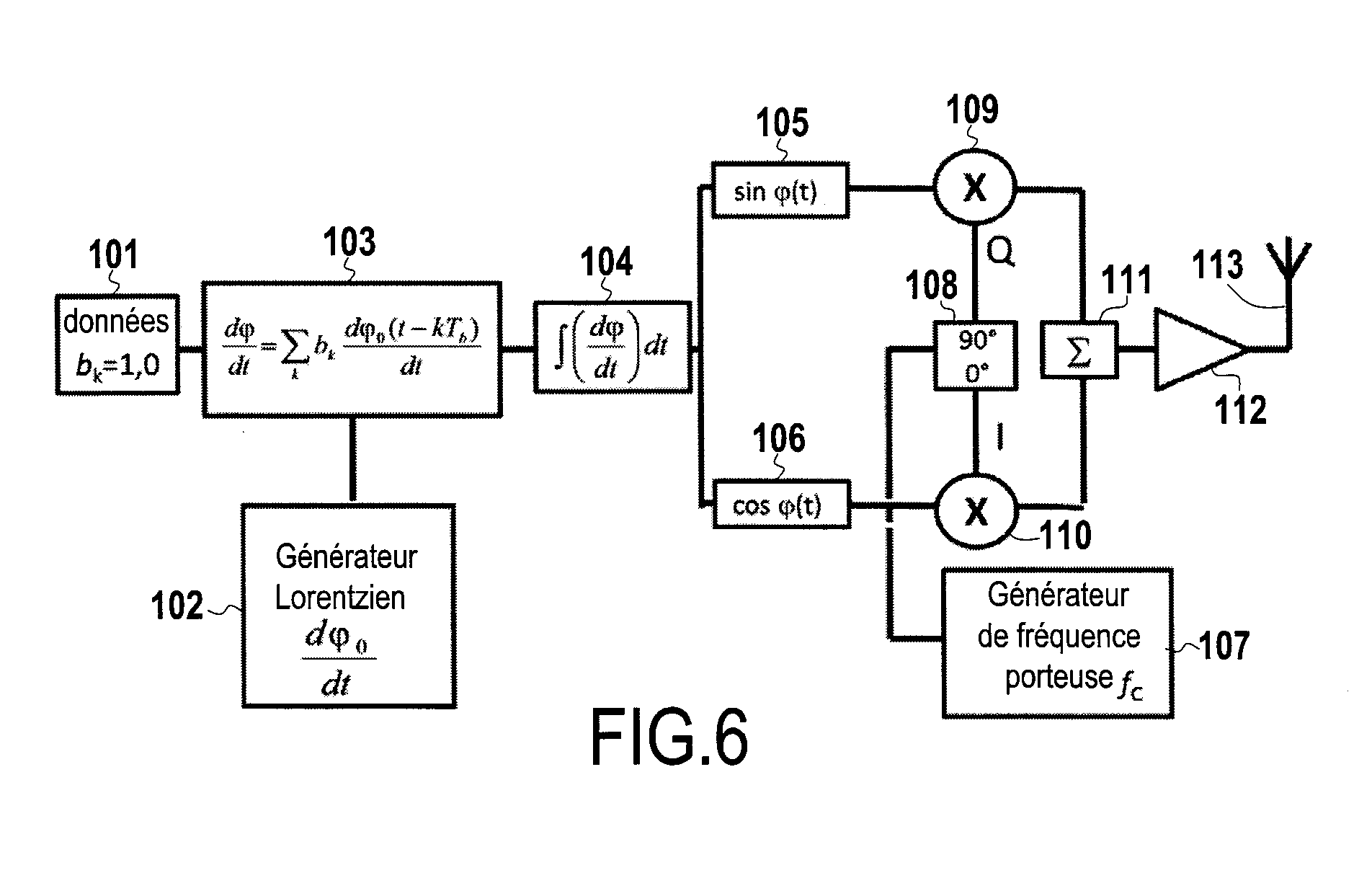
Le procédé de modulation de phase d'une onde porteuse est tel que l'on crée un ensemble de signaux sh (t) constitués d'une onde de fréquence porteuse fc dont la phase φ(t) =h φ0(t) est modulée dans le temps t de telle sorte que sh (t) = cos(2π fct+ h φ0 (t) ), où h est un nombre entier et où φ0(t) = 2 arctan((t - t0)/ w0). La modulation correspond à une impulsion de phase unique centrée au temps t0 de durée caractéristique w0 positive et incrémentant la phase du signal sh (t) de la quantité h 2 π, de telle sorte que l'on génère directement un spectre de fréquence à bande latérale unique. L'onde porteuse peut être de type électromagnétique ou de type acoustique. Le procédé s'applique notamment au transport d'une information binaire par codage de phase à bande latérale unique, à la génération de signaux orthogonaux à bande latérale unique, à la détection de signaux numériques multi-niveaux codés en phase à bande latérale unique, à l'émission en phase et hors phase de signaux binaires codés en phase à bande latérale unique, ainsi qu'à une modulation mixte amplitude-phase à bande latérale unique.
Method and device for phase modulation of a carrier wave and application to the detection of multi-level phase-encoded digital signals (WIPO link)
The method for phase modulation of a carrier wave involves creating a set of signals sh(t) constituted by a wave of carrier frequency fc of which the phase φ(t) = hφ0(t) is modulated in time t such that sh(t) = cos(2πfct+ hφ0(t)), where h is an integer and where φ0(t) = 2arctan((t - t0)/w0). The modulation corresponds to a single-phase pulse centred at time t0 with positive characteristic duration w0 and incrementing the phase of the signal sh(t) by the quantity h2π, in such a way as to directly generate a single-sideband frequency spectrum. The carrier wave can be electromagnetic or acoustic. The method can be applied, in particular, to the transport of a piece of binary information by single sideband phase encoding, to the generation of orthogonal single-sideband signals, to the detection of multi-level phase-encoded digital signals having a single sideband, to the in-phase and out-of-phase transmission of phase-encoded binary signals having a single sideband, and to a mixed amplitude/phase single-sideband modulation.
Contact : C. Glattli (IRAMIS/SPEC)
Numéro d’identification : WO/2016/139419 (lien OMPI)
Numéro d’identification CEA BD 15997
Année de dépôt : 03-03-2015
Date de publication : 09-09-2016
Procédé et dispositif de spectroscopie de résonance de spin électronique de tres haute sensibilité
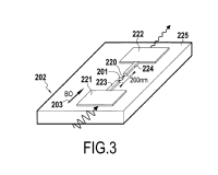
Le dispositif pour la détection et la caractérisation de spins électroniques dans un échantillon (201) comprend un micro-résonateur électromagnétique (202), ayant une fréquence de résonance cor dans le domaine micro-onde et un facteur de qualité Q et dans lequel est inséré l'échantillon (201); un dispositif de création d'un champ magnétique B0 dans l'échantillon (201) pour amener à résonance avec la fréquence de résonance cor une fréquence cos de transition des spins, telle que cos=yB0, où γ est un facteur gyromagnétique des spins; un dispositif de détection de spins recevant des signaux du micro-résonateur électromagnétique (202) associé à l'échantillon (201) et comprenant au moins un amplificateur bas-bruit fonctionnant à une température comprise entre 1 et 10 K et une série d'amplificateurs et un démodulateur fonctionnant à température ambiante. Le micro-résonateur électromagnétique (202) est en métal supraconducteur et est réalisé à l'échelle nanométrique en comprenant une zone active constituée par une constriction (220) essentiellement parallélépipédique, avec une épaisseur comprise entre 8 et 30 nm, une largeur comprise entre 10 et 500 nm et une longueur comprise entre 100 et 5000 nm. Le dispositif présente une sensibilité améliorée et permet l'analyse d'échantillons de très petite taille.
Method and device for very high sensitivity electron spin resonance spectroscopy (WIPO link)
The device for detecting and characterising electron spins in a sample (201) comprises an electromagnetic microresonator (202), having a resonant frequency cor in the microwave range and a quality factor Q and into which the sample (201) is inserted; a device for creating a magnetic field B0 in the sample (201) for bringing a spin transition frequency cos into resonance with the resonant frequency cor, such that cos = yB0, where γ is a gyromagnetic factor of the spins; a spin detection device receiving signals from the electromagnetic microresonator (202) associated with the sample (201) and comprising at least one low-noise amplifier operating at a temperature of between 1 and 10 K and a series of amplifiers and a demodulator operating at ambient temperature. The electromagnetic microresonator (202) is made from superconducting metal and is produced on the nanometre scale, comprising an active area formed by a substantially parallelepiped constriction (220), with a thickness of between 8 and 30 nm, a width of between 10 and 500 nm and a length of between 100 and 5000 nm. The device has improved sensitivity and allows samples of a very small size to be analysed.
Contact : P. Bertet.
