On January 6, 2014, the teams of the SPCSI (Division of Physics and Chemistry of Surfaces and Interfaces) have been officially associated to IRAMIS/NIMBE (chemists) and IRAMIS/SPEC (physicists).
Since july 2000 to the end of 2013, the SPCSI (Physics and Chemistry of Surfaces and Interfaces Laboratory) has been a research unit for the studies of basic properties of surfaces and interfaces and their potential applications. This Laboratory was part of to the Research Division on Atoms, Molecules and Condensed Matter (DRECAM) then IRAMIS (Saclay Institute of Matter and Radiation) within the Department of Matter Sciences (DSM) of the CEA (French Atomic Energy Commission).
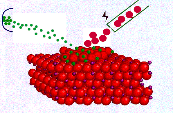
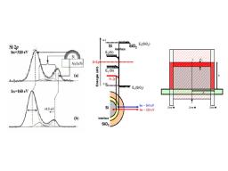
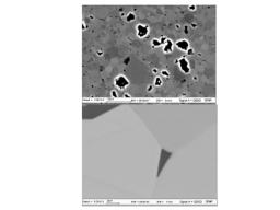
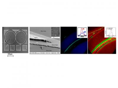
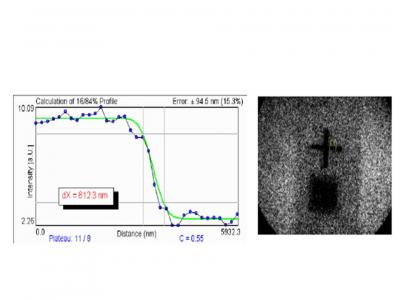
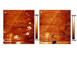
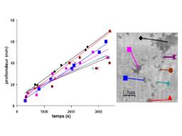
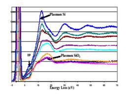
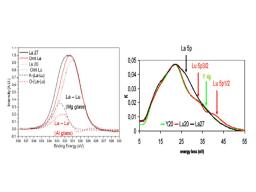
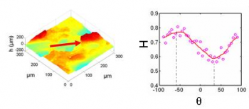
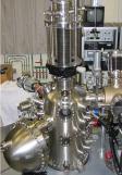
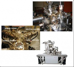
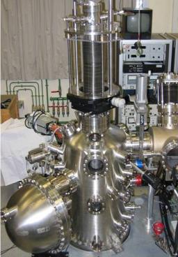
Gathering chemists and physicists, the SPCSI was equipped with a powerful set of devices for characterization at the atomic scale of surfaces: an XPS Kratos and a platform of equipments (STM / AFM - LEEM / PEEM - XPD) to investigate surfaces under ultrahigh vacuum, that the NIMBE and SPEC teams continue today to use successfully.
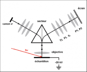
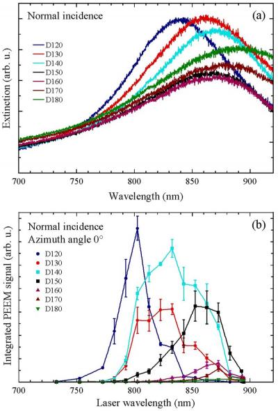
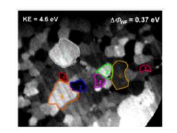
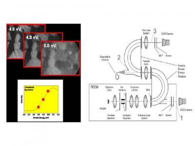
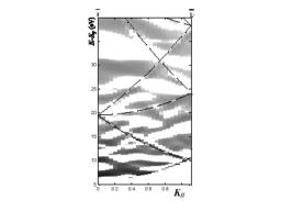
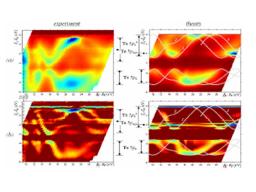
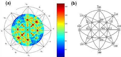
Development of novel XPEEM (spatial,momentum and energy resolved)
Development of novel XPEEM (spatial,momentum and energy resolved)


Vous devez préciser l'id_ast dans la table des unités.