


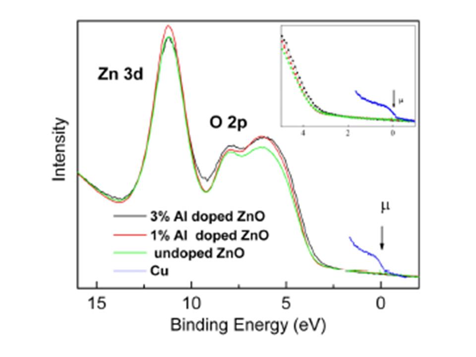
Fig. 1:the valence band at h ν=35 eV for 1 and 3% Al doped samples. The chemical potential μ measured from a copper foil in electrical contact with the sample is shown. Inset: Close-up of valence band edge.
Transparent conductive oxide (TCO) films have been extensively used in optoelectronic devices because of their high visible transmittance and low DC resistivity. ZnO has appropriate optical transparency and small reflectance at 600 nm, the optimal wavelength for the silicon solar cells [1], can be used as the passivation layer of the active Si electrode and is naturally abundant and non toxic. The use of a single layer acting simultaneously as the antireflection coating, the passivation layer and the electrode for extracting the electrons from the photovoltaic cell, could be a real breakthrough in the solar cell technology, simplifying fabrication and reducing costs. Spray pyrolysis is an interesting alternative method to obtain TCO coatings because of its simplicity: it can coat extended surfaces; does not need high vacuum, and is easily inserted in a production line. [2]
Increases in conductivity of several orders of magnitude have been observed when doping ZnO films with a group III element up to a [Al]/[Zn] = 3% atomic ratio. An open question is the conduction mechanism compared to undoped films.
Resistivity of the films was determined using Van der Pauw’s method. A decrease of resistivity in two orders of magnitude is measured for 3% Al doping. The high resolution valence-band PES spectra using 35eV photons are shown in Fig. 1 (right). [3] None of the samples present a density of states in the band gap region. We observe a slight reduction of the band gap compared to the 1% and the undoped samples. The band gap is reduced by ~150 meV. This is interpreted as a result of the hybridization between the Al-dopants with the O atoms in the ZnO. A slight decrease of the optical band-gap (~ 90 meV) is also measured in transmittance measurements. [4] No insulator-metal transition is observed. Conductivity occurs principally via a band conduction mechanism. The conductivity jump is described in terms of a Vervey transition.[5] The independent variable is the Al doping, giving discontinuity in the first derivative of Gibb’s function Δσ/ΔND. ΔVBM = 150 meV
leads to a decrease ΔEA in the activation energy for electrons to accede to the conduction band. Thus the conductivity jump Δσ can be written as Δσ ≈ exp (150/kT) = 378, similar to the electrical measurements.
REFERENCES :
[1] J.J. Aranovich et al., J. Appl.Phys. 51, 4260-4268 (1980)
[2] H. Mondragón-Suárez et al., Appl. Surf. Sci. 193, 52-59 (2002)
[3] M. Addou et al., J. Chim. Phys. Phys.Chim. Biol. 96, 232-244 (1999)
[4] J.H. Park et al., Phys. Rev. B 55, 12813-12817 (1997)
• ![]() Les archives de l'IRAMIS et du DRECAM / Archives of DRECAM and IRAMIS › Surfaces and nanostructures
Les archives de l'IRAMIS et du DRECAM / Archives of DRECAM and IRAMIS › Surfaces and nanostructures ![]() Physique, chimie, nanosciences et matériaux autour des grands instruments
Physique, chimie, nanosciences et matériaux autour des grands instruments
• Laboratory of Physics and Chemistry of Surfaces and Interfaces • Service de Physique et Chimie des Surfaces et des Interfaces
• Laboratory of Nanostructures Studies and Surface Imagery (LENSIS) • Laboratoire d'Etude des NanoStructures et Imagerie de Surface (LENSIS)
