

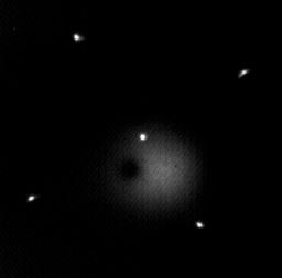
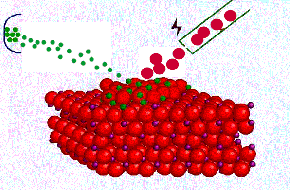
Les techniques de diffraction permettent de sonder l'ordre dans la matière. Pour ceci, on fait interagir une onde dont la longueur d'onde λ est comparable à la taille du motif cristallin élémentaire de l'échantillon. Ce peut être une onde électromagnétique (rayons X, lumière Laser) ou des particules (électrons, neutrons ou des atomes d'hélium).
Plusieurs types de microscopies électroniques sont disponibles à l'IRAMIS :
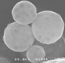
- Microscopie à transmission (TEM : Transmission Electron Microscope), qui permet d'atteindre les plus hautes résolutions par diffusion/difffraction d'un faisceau d'électrons à travers un échantillon ultra-mince
- Microscopie MEB et MEB-FEG (SPAM et SIS2M), ou microscopie à balayage, pour laquelle un faisceau d'électrons balaye la surface de l'échantillon permettant d'obtenir une image de sa surface.
Development of novel XPEEM (spatial,momentum and energy resolved)
L'éclairement, par un rayonnement suffisamment énergétique, de la surface d'un matériau peut conduire à l'émission d'électrons dont la spectroscopie (étude en énergie) apporte des informations sur la composition de la surface étudiée.
Development of novel XPEEM (spatial,momentum and energy resolved)
A phenomenon of transport is due to a force whose origin can be varied (electric or magnetic field, gradient of concentration, pressure etc...). Under the heading "transport measurements" are gathered various associated measurement techniques which can be flux measurements (heat, particles, electrical current, etc...), or statistical methods.

The nanotechnologies require to build complex heterostructures at an atomic scale. Those are generally carried out by deposition on a substrate (metal or oxide). The control of the physical phenomena of the growth and the realization of dots or thin films of well defined structure is one of the keys of the realization of new devices with new properties. The teams of the DRECAM largely use the various techniques of deposition, control of the growth and analyses and contribute to develop them.
Near field microscopies cover a whole of techniques making it possible to visualize the surface of materials at a nanometric scale.
These microscopies gather:
- Scanning Tunneling Microscopy (STM)
- Atomic Force Microscopy (AFM)
- Magnetic Force Microscopy (MFM)
All these techniques have in common the positioning nanometric of a tip on top of the sample whose position is controlled according to the selected signal (current, force).

The magnetic properties of bulk samples and thin films can be studied by Vibrating Sample Magnetometry (VSM) or Magneto-optic Kerr effect (MOKE).
Two VSM measuring devices are available in the IRAMIS:
- One device in SPEC
- One device in SPCSI
For research on low TC superconductors or more generally on electronic and magnetic matter properties at very low temperature, specific equipments are developped, like a dilution-fridge equipped SQUID magnetometer.
x-rays, electromagnetic radiation beyond the remote ultraviolet ray, cover a range wavelength around the tenth of nanometer. This distance is about the distance between atoms in the condensed matter. The diffraction of x-rays thus makes it possible to probe the matter, and to obtain information on the structure, the order and the composition of materials.