

X-ray Photoelectron Spectroscopy (XPS)
XPS, X-ray Photoelectron Spectroscopy is a surface analysis technique which provides both chemical and electronic properties. Through the photoelectric effect, photoelectrons are ejected from the surface illuminated with a X-ray source. They have characteristic binding energy which depends on the element, orbital and chemical environment of the atom.
This technique allows the detection of virtually all elements present on the surface (probing depth 1 to 10nm).
In the context of our laboratory studies, XPS is particularly suitable for the identification of chemical bonds showing the functionalization of surfaces and materials and for the calculation of stoichiometric ratios of thin layers.
Our laboratory is equipped with a Kratos Axis Ultra DLD (http://www.kratos.com/products/axis-ultra-dld)
This equipement is open to intra- and extra-IRAMIS collaborations.
Contact: Jocelyne Leroy
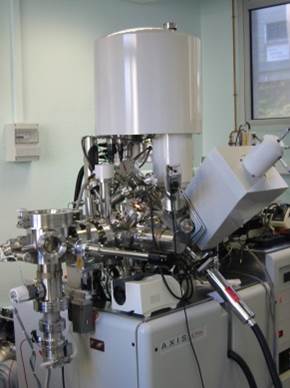
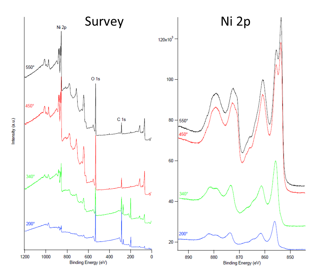
Figure: Example of survey and Ni2p XPS spectra of inkjet printed NiO films annealed at different temperatures
2D/3D Printing technologies and Spray
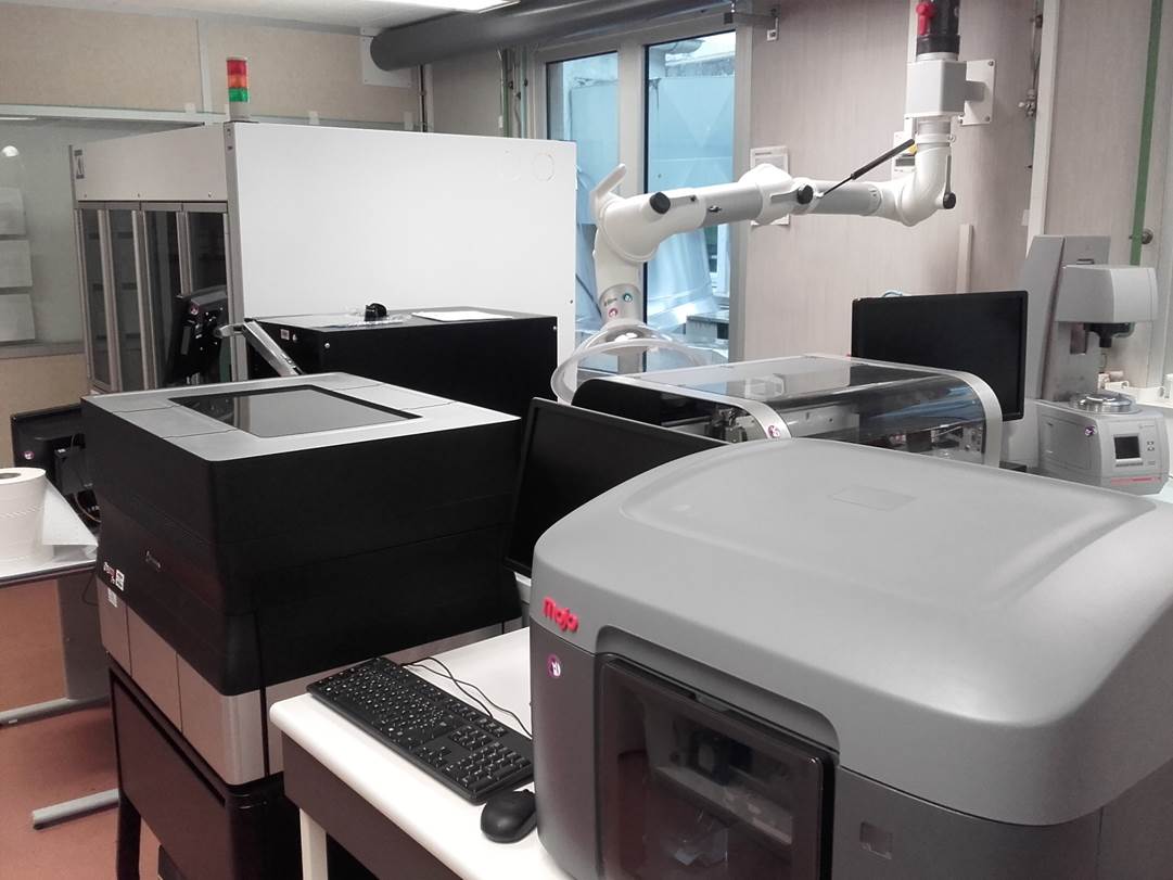
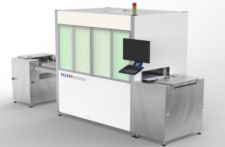
LICSEN progressively assembled a set of printing equipments devoted to its activities in the field of bio-sensors (lab on paper). organic electronics (antenna), surface modifications (metallization of plastics), microfluidics and energy-related materials. It notably includes a Kelenn Technology K-SCAN printer, a Dimatix 2D printer, a Stratasys Object30Pro, several tabletop 3D printers, a spray system, several photonic curing systems...
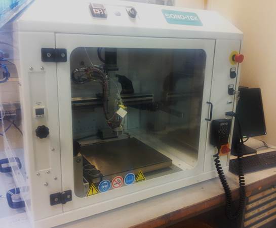
Contact 2D/3D printing : Fanny Hauquier
Contact Spray: Bruno Jousselme.
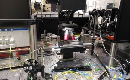
Electrochemical Microscopy (SECM)
SECM is a powerfull tool for the study of the local electrochemical properties of surfaces and nano-materials. It is also a versatile technique for local surface modification (electrograffting, functionnalization, local oxidation/reduction...).
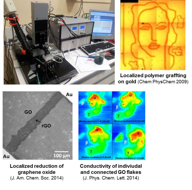
Contact: Renaud Cornut
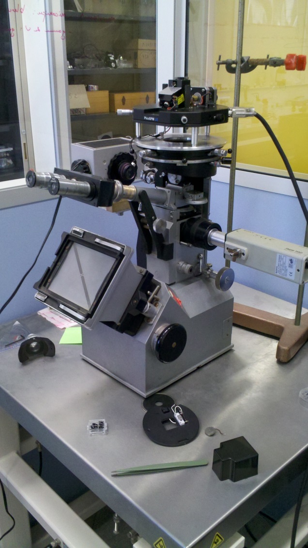
Electron-beam Litography and Nanofabrication
LICSEN is equipped for e-beam litography and has access to the clean room facility at CEA-SPEC (optical litography, wet and dry etching...). We also operate several SEMs and AFMs.
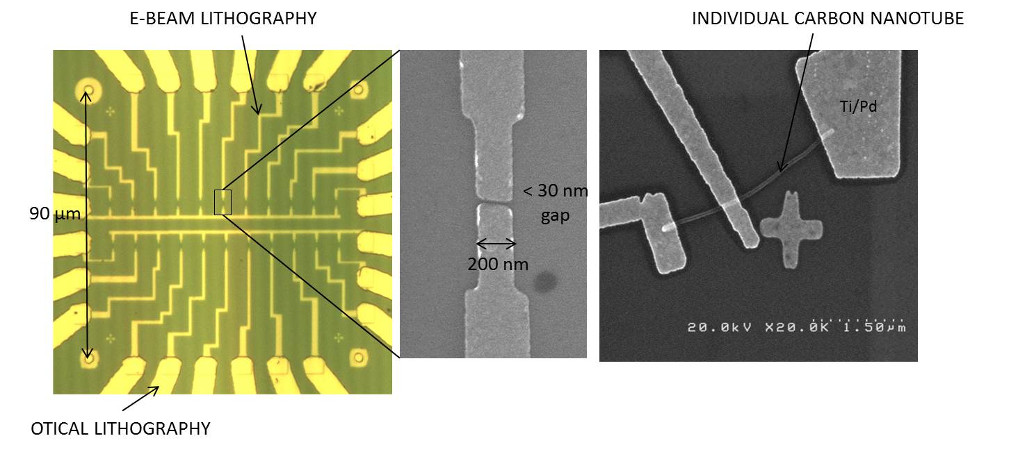
Contact: Vincent Derycke
Organic Electronic (oPV & oTFT) Fabrication & Characterization
An optical bench composed of a solar simulator (Xe lamp), monochromator and powermeter is coupled to a micro-probe station to characterize photovoltaic and organic field effect transistor (OFET). Both are integrated into a controlled atmosphere series of glove boxes which also content a thermal evaporator and a spincoater.
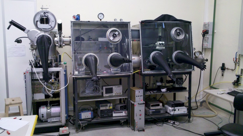
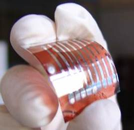
The lab is also equipped with several atomic force microscopes (AFMs). Amung them one has been set onto an inverse microscope to allow electrical measurements upon light exposure an is particularily dedicated to organic electronic samples (oPV layers). This homemade set-up also allows a top or bottom view of the scanned area.
Contact: Ludovic Tortech
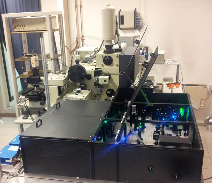
Raman spectroscopy & Optoelectronics
Raman spectroscopy is a central tool for the study of carbon-material (CNTs, graphene) chemical functionnalization. Licsen notably operates a T64000 micro-raman with multiple sources covering a wide range of approriate wavelenghts.
In addition, LICSEN is also equiped for visible and near infrared optoelectronics. This notably allows studying the optoelectronic properties (electroluminescence and photodetection) of carbon nanotube-based devices and their coupling with integrated silicon waveguides.
Contact: Arianna Filoramo
