


Drawing obtained by locally grafting vinyl monomers on gold with the Elec Draw device (image size 200 m).
The development and implementation of micro- and bio-electronic devices often need the deposition of layers of organic substances on conductive or semiconducting surfaces. In that aim, surface chemical reactions (or grafting) are very effective. The miniaturization of electronic components requires the realization of a very localized grafting, at the micron and even sub-micron scale.
To graft locally a molecule onto a surface, the macroscopic surface of a substrate is usually exposed to very small quantities of solution. The localization can be also assisted by a light beam or a catalyst. Most of these techniques require a multiple step processes and their implementation is usually tedious and expensive. In this context, we show that it is possible through an original approach to make a local grafting in one single step, requiring no masking technique and by light and low cost technologies.
We have shown recently [1-4] that it was already possible to decorate, in one step and locally, by an organic film (electro-grafting of vinyl monomers), the surface of a sample with different zones of conductivity (Au / Si, Si / Si-doped). The spatial selectivity of the deposit is obtained simply in that case by playing on the imposed bias voltage, to promote the electronic transfer (and thus the grafting of the polymer) to one surface to the exclusion of another. The predefined pattern is perfectly respected, with a lateral resolution limited only by the thickness of the film (a few nm to few hundred nm).
Our recent results in that field concern the extension of the localized functionalization process to surfaces of initially homogeneous conductors or semiconductors, i.e. without predefined patterns. In these conditions, the localization of the grafting may be obtained from the selectivity offered, either by light (photo-localization on photosensitive substrates), [5] or by the electric field in the environment of an electrochemical microscope.
The latest can be explored by combining the techniques of local probe, derived from an electrochemical microscope (SECM) with those of an electrochemical AFM mode (AFM-SECM), and those of electro-grafting of vinyl monomers. The grafting reaction is initiated by aryl radicals from the aqueous electrochemical reduction of diazonium salts. The location of grafting can be controlled by finely adjusting all parameters: probe-substrate distance, current density and reaction time.
The use of these electrochemical microscopies allowed to "print" plots, lines, or complex figures on initially homogeneous conducting substrates with a lateral resolution of about one to two times the size of the probe. Lower size may be expected by improving the shape of AFM-SECM tips. The resolution thus obtained is quite comparable to other competitive methods of nano-fabrication based on soft lithography technology (nano-printing (such as rubber stamp), nano-compression (pressing into a mould) or dip-pen and in particular also compatible with most developed micro-systems for biology. It is a rapid (a few hundred milliseconds to seconds, depending on the complexity of the pattern), easy to implement and allows for decorating various substrates with an adjustable thread.
The electrochemical microscopy associated with a local probe thus becomes a real tool for local electrochemical lithography that opens the way for processes at the micro / nano-scale of any conductor or semiconductor substrate. This work has been the subject of a recent publication in ChemPhysChem [6].
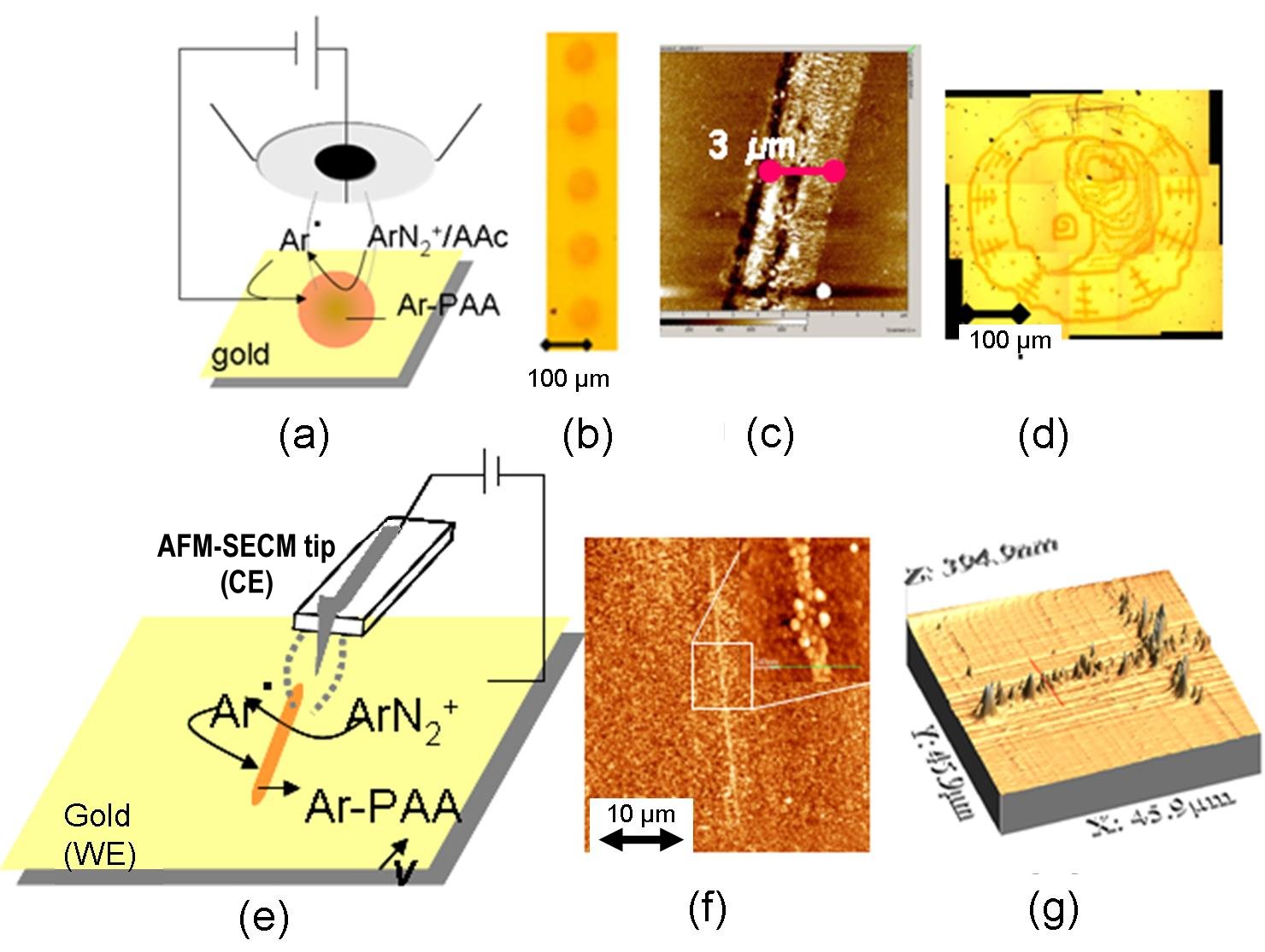
Schematic diagrams of the SECM (a) and SECM-AFM (e) electro-grafting processes. (b-d): plots, lines and structures made with a SECM probe, (f-g) lines obtained by electrochemical lithography (resolution <150 nm) performed using the AFM-SECM tip.
References:
[1] Mask-free Localized Grafting of Organic Polymers at the Micrometer or Submicrometer Scale on Composite Conductors or Semiconductor Substrates,
J. Charlier, S. Ameur, J. P. Bourgoin, C. Bureau and S. Palacin, Adv. Funct. Mater. 14 (2004) 125.
[2] Directed Organic Grafting on Locally Doped Silicon Substrates,
J. Charlier, L. Baraton, C. Bureau and S. Palacin, ChemPhysChem 6 (2005) 70.
[3] Selectivity of organic grafting as a function of the nature of semiconducting substrates,
J. Charlier, E. Clolus, C. Bureau and S. Palacin, J. Electroanal. Chem. 625 (2009) 97.
[4] Local silicon doping as a promoter of patterned electrografting of diazonium for directed surface functionalization,
J. Charlier, S. Palacin, J. Leroy, D. Del Frari, L. Zagonel, N. Barrett, O. Renault, A. Bailly and D. Mariolle, J. Mater. Chem. 18 (2008) 3136.
[5] Localized organic grafting on photosensitive semiconductors substrates,
J. Charlier, E. Clolus, C. Bureau and S. Palacin, J. Electroanal. Chem. 622 (2008) 238.
![]() [
[
6] Localized Electrografting of Vinylic Monomers on a Conducting Substrate by Means of an Integrated Electrochemical AFM Probe,
A. Ghorbal, F. Grisotto, J. Charlier, S. Palacin, C. Goyer and C. Demaille, ChemPhysChem 2009, in press.

• ![]() Les archives de l'IRAMIS et du DRECAM / Archives of DRECAM and IRAMIS › Surfaces and nanostructures
Les archives de l'IRAMIS et du DRECAM / Archives of DRECAM and IRAMIS › Surfaces and nanostructures
• Laboratory of Physics and Chemistry of Surfaces and Interfaces
